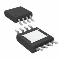
LTC3631IMS8E#TRPBF Linear Technology, LTC3631IMS8E#TRPBF Datasheet - Page 8

LTC3631IMS8E#TRPBF
Manufacturer Part Number
LTC3631IMS8E#TRPBF
Description
IC CONV STP-DWN SYNC ADJ 8-MSOP
Manufacturer
Linear Technology
Type
Step-Down (Buck)r
Datasheet
1.LTC3631EMS8E-5PBF.pdf
(22 pages)
Specifications of LTC3631IMS8E#TRPBF
Internal Switch(s)
Yes
Synchronous Rectifier
Yes
Number Of Outputs
1
Voltage - Output
0.8 ~ 45 V
Current - Output
100mA
Voltage - Input
4.5 ~ 45 V
Operating Temperature
-40°C ~ 125°C
Mounting Type
Surface Mount
Package / Case
8-MSOP Exposed Pad, 8-HMSOP, 8-eMSOP
Lead Free Status / RoHS Status
Lead free / RoHS Compliant
Power - Output
-
Frequency - Switching
-
Available stocks
Company
Part Number
Manufacturer
Quantity
Price
operaTion
LTC3631
The LTC3631 is a step-down DC/DC converter with internal
power switches that uses Burst Mode control, combining
low quiescent current with high switching frequency,
which results in high efficiency across a wide range of
load currents. Burst Mode operation functions by using
short “burst” cycles to ramp the inductor current through
the internal power switches, followed by a sleep cycle
where the power switches are off and the load current is
supplied by the output capacitor. During the sleep cycle,
the LTC3631 draws only 12µA of supply current. At light
loads, the burst cycles are a small percentage of the total
cycle time which minimizes the average supply current,
greatly improving efficiency.
Main Control Loop
The feedback comparator monitors the voltage on the V
pin and compares it to an internal 800mV reference. If
this voltage is greater than the reference, the comparator
activates a sleep mode in which the power switches and
current comparators are disabled, reducing the V
supply current to only 12µA. As the load current discharges
the output capacitor, the voltage on the V
When this voltage falls 5mV below the 800mV reference,
the feedback comparator trips and enables burst cycles.
At the beginning of the burst cycle, the internal high side
power switch (P-channel MOSFET) is turned on and the
inductor current begins to ramp up. The inductor current
increases until either the current exceeds the peak current
comparator threshold or the voltage on the V
exceeds 800mV, at which time the high side power switch
is turned off, and the low side power switch (N-channel
MOSFET) turns on. The inductor current ramps down until
the reverse current comparator trips, signaling that the
current is close to zero. If the voltage on the V
still less than the 800mV reference, the high side power
switch is turned on again and another cycle commences.
The average current during a burst cycle will normally be
8
(Refer to Block Diagram)
FB
pin decreases.
FB
FB
IN
pin is
pin
pin
FB
greater than the average load current. For this architecture,
the maximum average output current is equal to half of
the peak current.
The hysteretic nature of this control architecture results
in a switching frequency that is a function of the input
voltage, output voltage and inductor value. This behavior
provides inherent short-circuit protection. If the output
is shorted to ground, the inductor current will decay very
slowly during a single switching cycle. Since the high side
switch turns on only when the inductor current is near
zero, the LTC3631 inherently switches at a lower frequency
during start-up or short-circuit conditions.
Start-Up and Shutdown
If the voltage on the RUN pin is less than 0.7V, the LTC3631
enters a shutdown mode in which all internal circuitry is
disabled, reducing the DC supply current to 3µA. When the
voltage on the RUN pin exceeds 1.21V, normal operation of
the main control loop is enabled. The RUN pin comparator
has 110mV of internal hysteresis, and therefore must fall
below 1.1V to disable the main control loop.
The HYST pin provides an added degree of flexibility for
the RUN pin operation. This open-drain output is pulled
to ground whenever the RUN comparator is not tripped,
signaling that the LTC3631 is not in normal operation. In
applications where the RUN pin is used to monitor the
V
pin can be used to increase the effective RUN comparator
hysteresis.
An internal 1ms soft-start function limits the ramp rate of
the output voltage on start-up to prevent excessive input
supply droop. If a longer ramp time and consequently less
supply droop is desired, a capacitor can be placed from the
SS pin to ground. The 5µA current that is sourced out of
this pin will create a smooth voltage ramp on the capacitor.
If this ramp rate is slower than the internal 1ms soft-start,
IN
voltage through an external resistive divider, the HYST
3631fc


