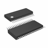
LTC3855EFE#TRPBF Linear Technology, LTC3855EFE#TRPBF Datasheet - Page 27

LTC3855EFE#TRPBF
Manufacturer Part Number
LTC3855EFE#TRPBF
Description
IC CTLR DC/DC DUAL 2PH 38TSSOP
Manufacturer
Linear Technology
Series
PolyPhase®r
Type
Step-Down (Buck)r
Datasheet
1.LTC3855EUJPBF.pdf
(44 pages)
Specifications of LTC3855EFE#TRPBF
Internal Switch(s)
No
Synchronous Rectifier
Yes
Number Of Outputs
2
Voltage - Output
0.6 ~ 3.3 V, 0.6 ~ 12.5 V
Current - Output
25A
Frequency - Switching
250kHz ~ 770kHz
Voltage - Input
4.5 ~ 38 V
Operating Temperature
-40°C ~ 85°C
Mounting Type
Surface Mount
Package / Case
38-TSSOP Exposed Pad, 38-eTSSOP, 38-HTSSOP
Lead Free Status / RoHS Status
Lead free / RoHS Compliant
Power - Output
-
Available stocks
Company
Part Number
Manufacturer
Quantity
Price
applicaTions inForMaTion
Phase-Locked Loop and Frequency Synchronization
The LTC3855 has a phase-locked loop (PLL) comprised of
an internal voltage-controlled oscillator (V
detector. This allows the turn-on of the top MOSFET of
controller 1 to be locked to the rising edge of an external
clock signal applied to the MODE/PLLIN pin. The turn-on
of controller 2’s top MOSFET is thus 180 degrees out-
of-phase with the external clock. The phase detector is
an edge sensitive digital type that provides zero degrees
phase shift between the external and internal oscillators.
This type of phase detector does not exhibit false lock to
harmonics of the external clock.
The output of the phase detector is a pair of complementary
current sources that charge or discharge the internal filter
network. There is a precision 10µA of current flowing out
of FREQ pin. This allows the user to use a single resistor
to SGND to set the switching frequency when no external
clock is applied to the MODE/PLLIN pin. The internal switch
between FREQ pin and the integrated PLL filter network
is ON, allowing the filter network to be pre-charged to the
same voltage potential as the FREQ pin. The relationship
between the voltage on the FREQ pin and the operating
frequency is shown in Figure 12 and specified in the Elec-
trical Characteristic table. If an external clock is detected
on the MODE/PLLIN pin, the internal switch mentioned
above will turn off and isolate the influence of FREQ pin.
Note that the LTC3855 can only be synchronized to an
external clock whose frequency is within range of the
LTC3855’s internal V
250kHz and 770kHz. A simplified block diagram is shown
in Figure 13.
If the external clock frequency is greater than the internal
oscillator’s frequency, f
ously from the phase detector output, pulling up the filter
network. When the external clock frequency is less than f
current is sunk continuously, pulling down the filter network. If
the external and internal frequencies are the same but exhibit
a phase difference, the current sources turn on for an amount
of time corresponding to the phase difference. The voltage on
the filter network is adjusted until the phase and frequency of
the internal and external oscillators are identical. At the stable
operating point, the phase detector output is high impedance
and the filter capacitor holds the voltage.
CO
OSC
. This is guaranteed to be between
, then current is sourced continu-
CO
) and a phase
OSC
,
Typically, the external clock (on MODE/PLLIN pin)
input high threshold is 1.6V, while the input low threshold
is 1V. It is not recommended to apply the external clock
when IC is in shutdown.
Minimum On-Time Considerations
Minimum on-time t
that the LTC3855 is capable of turning on the top MOSFET.
It is determined by internal timing delays and the gate
charge required to turn on the top MOSFET. Low duty
cycle applications may approach this minimum on-time
limit and care should be taken to ensure that
OSCILLATOR
EXTERNAL
t
ON(MIN)
Figure 12. Relationship Between Oscillator
Frequency and Voltage at the FREQ Pin
Figure 13. Phase-Locked Loop Block Diagram
900
800
700
600
500
400
300
200
100
MODE/
PLLIN
<
0
0
V
V
IN
OUT
(f)
FREQUENCY
DETECTOR
0.5
ON(MIN)
DIGITAL
PHASE/
FREQ PIN VOLTAGE (V)
1
is the smallest time duration
SYNC
1.5
2.4V 5V
2
LTC3855
10µA
3855
2.5
F12
FREQ
R
SET
VCO
3855 F13
3855f


