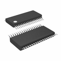
LTC3855EFE#TRPBF Linear Technology, LTC3855EFE#TRPBF Datasheet - Page 32

LTC3855EFE#TRPBF
Manufacturer Part Number
LTC3855EFE#TRPBF
Description
IC CTLR DC/DC DUAL 2PH 38TSSOP
Manufacturer
Linear Technology
Series
PolyPhase®r
Type
Step-Down (Buck)r
Datasheet
1.LTC3855EUJPBF.pdf
(44 pages)
Specifications of LTC3855EFE#TRPBF
Internal Switch(s)
No
Synchronous Rectifier
Yes
Number Of Outputs
2
Voltage - Output
0.6 ~ 3.3 V, 0.6 ~ 12.5 V
Current - Output
25A
Frequency - Switching
250kHz ~ 770kHz
Voltage - Input
4.5 ~ 38 V
Operating Temperature
-40°C ~ 85°C
Mounting Type
Surface Mount
Package / Case
38-TSSOP Exposed Pad, 38-eTSSOP, 38-HTSSOP
Lead Free Status / RoHS Status
Lead free / RoHS Compliant
Power - Output
-
Available stocks
Company
Part Number
Manufacturer
Quantity
Price
LTC3855
applicaTions inForMaTion
This occurs around 50% duty cycle on either channel due
to the phasing of the internal clocks and may cause minor
duty cycle jitter.
Reduce V
of the regulator in dropout. Check the operation of the
undervoltage lockout circuit by further lowering V
monitoring the outputs to verify operation.
Investigate whether any problems exist only at higher out-
put currents or only at higher input voltages. If problems
coincide with high input voltages and low output currents,
look for capacitive coupling between the BOOST, SW, TG,
and possibly BG connections and the sensitive voltage
and current pins. The capacitor placed across the current
sensing pins needs to be placed immediately adjacent to
the pins of the IC. This capacitor helps to minimize the
effects of differential noise injection due to high frequency
capacitive coupling. If problems are encountered with
high current output loading at lower input voltages, look
for inductive coupling between C
MOSFET components to the sensitive current and voltage
sensing traces. In addition, investigate common ground
path voltage pickup between these components and the
SGND pin of the IC.
Design Example
As a design example for a two channel high current regula-
tor, assume V
V
(see Figure 16).
The regulated output voltages are determined by:
Using 20k 1% resistors from both V
the top feedback resistors are (to the nearest 1% standard
value) 40.2k and 20k.
The frequency is set by biasing the FREQ pin to 1V (see
Figure 12).
The inductance values are based on a 35% maximum
ripple current assumption (5.25A for each channel). The
highest value of ripple current occurs at the maximum
OUT1
V
OUT
= 1.8V, V
= 0.6V • 1+
IN
from its nominal level to verify operation
IN
OUT2
= 12V(nominal), V
= 1.2V, I
R
R
B
A
MAX1,2
IN
, Schottky and the top
= 15A, and f = 400kHz
IN
FB
= 20V(maximum),
nodes to ground,
IN
while
input voltage:
Channel 1 will require 0.78µH, and channel 2 will require
0.54µH. The Vishay IHLP4040DZ-01, 0.56µH inductor is
chosen for both rails. At the nominal input voltage (12V),
the ripple current will be:
Channel 1 will have 6.8A (46%) ripple, and channel 2 will
have 4.8A (32%) ripple. The peak inductor current will be
the maximum DC value plus one-half the ripple current,
or 18.4A for channel 1 and 17.4A for channel 2.
The minimum on-time occurs on channel 2 at the maximum
V
With I
can be calculated by using the minimum value for the
maximum current sense threshold (45mV).
The equivalent required R
nel 1 and 2.6mΩ for channel 2. The DCR of the 0.56µH
inductor is 1.7mΩ typical and 1.8mΩ maximum for a
25°C ambient. At 100°C, the estimated maximum DCR
value is 2.3mΩ. The maximum DCR value is just slightly
under the equivalent R
required to divide down the signal.
For each channel, 0.1µF is selected for C1.
Choose R1 = 3.09k
IN
L
R
R1=
∆I
t
, and should not be less than 90ns:
ON(MIN)
SENSE(EQUIV)
=
L NOM
(
LIM
f •
(DCR
floating, the equivalent R
V
∆
)
=
OUT
=
I
MAX
L MAX
V
(
V
IN(MAX)
f
OUT
V
•
=
OUT
at 25°C) • C1
L
L
)
I
LOAD(MAX)
1
1
SENSE
f
−
−
=
V
SENSE
V
V
SENSE(MIN)
20V(400kHz)
IN NOM
IN MAX
V
V
values. Therefore, R2 is not
OUT
(
OUT
(
+
=
1.2V
value is 2.4mΩ for chan-
1.8mΩ • 0.1µF
∆I
)
)
L(NOM)
SENSE
0.56µH
2
= 150ns
resistor value
= 3.11k
3855f


