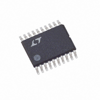
LTC3417AIFE-1#PBF Linear Technology, LTC3417AIFE-1#PBF Datasheet - Page 2

LTC3417AIFE-1#PBF
Manufacturer Part Number
LTC3417AIFE-1#PBF
Description
IC BUCK SYNC ADJ 1A/1.5A 20TSSOP
Manufacturer
Linear Technology
Type
Step-Down (Buck)r
Datasheet
1.LTC3417AEDHC-1PBF.pdf
(20 pages)
Specifications of LTC3417AIFE-1#PBF
Internal Switch(s)
Yes
Synchronous Rectifier
Yes
Number Of Outputs
2
Voltage - Output
0.8 ~ 5 V
Current - Output
1A, 1.5A
Frequency - Switching
1.5MHz, 0.6MHz ~ 4MHz
Voltage - Input
2.25 ~ 5.5 V
Operating Temperature
-40°C ~ 125°C
Mounting Type
Surface Mount
Package / Case
20-TSSOP Exposed Pad, 20-eTSSOP, 20-HTSSOP
Lead Free Status / RoHS Status
Lead free / RoHS Compliant
Power - Output
-
ABSOLUTE MAXIMUM RATINGS
LTC3417A-1
V
SYNC/MODE, SW1, SW2, RUN1,
RUN2, V
I
V
LEAD FREE FINISH
LTC3417AEDHC-1#PBF
LTC3417AIDHC-1#PBF
LTC3417AEFE-1#PBF
LTC3417AIFE-1#PBF
Consult LTC Marketing for parts specifi ed with wider operating temperature ranges. *The temperature grade is identifi ed by a label on the shipping container.
Consult LTC Marketing for information on non-standard lead based fi nish parts.
For more information on lead free part marking, go to:
For more information on tape and reel specifi cations, go to:
ELECTRICAL CHARACTERISTICS
temperature range, otherwise specifi cations are at T
SYMBOL
V
I
PIN CONFIGURATION
ORDER INFORMATION
2
FB1
TH1
IN1
IN1
IN1
, I
, V
, I
, V
FB2
– V
IN2
TH2
IN2
IN2
FB1
Voltages........ –0.3V to ((V
Voltages ...................................... – 0.3V to 6V
, V
, V
IN2
FB2
PARAMETER
Operating Voltage Range
Feedback Pin Input Current
EXPOSED PAD (PIN 17) IS PGND2/GNDD
– V
, PHASE, FREQ,
RUN1
RUN2
16-LEAD (5mm × 3mm) PLASTIC DFN
I TH1
V
V
V
V
I
TH2
FB1
FB2
IN1
IN2
T
MUST BE SOLDERED TO PCB
IN1
JMAX
1
2
3
4
5
6
7
8
TAPE AND REEL
LTC3417AEDHC-1#TRPBF
LTC3417AIDHC-1#TRPBF
LTC3417AEFE-1#TRPBF
LTC3417AIFE-1#TRPBF
.......................................... 0.3V
= 125°C, θ
DHC PACKAGE
TOP VIEW
17
JA
= 43°C/ W
16
15
14
13
12
11
10
9
PGND1
SW1
PHASE
GNDA
FREQ
POR
SW2
SYNC/MODE
IN1
or V
http://www.linear.com/leadfree/
IN2
http://www.linear.com/tapeandreel/
A
= 25°C. V
) + 0.3V)
CONDITIONS
V
V
PART MARKING*
3417A1
3417A1
LTC3417AFE-1
LTC3417AFE-1
IN1
IN
The
= 6V Pin Under Test = 3V
= V
(Note 1)
l
IN
IN2
denotes the specifi cations which apply over the full operating
= 3.6V unless otherwise specifi ed (Note 2).
POR Voltage ................................................ –0.3V to 6V
Operating Temperature Range (Note 2)
Junction Temperature (Notes 7, 8) ...................... 125°C
Storage Temperature Range ................... –65°C to 150°C
LTC3417AE-1 ...................................... –40°C to 85°C
LTC3417AI-1 ..................................... –40°C to 125°C
PACKAGE DESCRIPTION
16-Lead (3mm × 5mm) Plastic DFN
16-Lead (3mm × 5mm) Plastic DFN
20-Lead Plastic TSSOP
20-Lead Plastic TSSOP
PGND2
GNDD
RUN1
RUN2
EXPOSED PAD (PIN 21) IS PGND2/GNDD
V
V
V
V
I
I
TH1
TH2
FB1
FB2
IN1
IN2
T
MUST BE SOLDERED TO PCB
20-LEAD PLASTIC TSSOP
JMAX
10
1
2
3
4
5
6
7
8
9
= 125°C, θ
FE PACKAGE
TOP VIEW
21
JA
MIN
2.25
= 38°C/ W
20
19
18
17
16
15
14
13
12
11
GNDD
PGND1
SW1
PHASE
GNDA
FREQ
POR
SW2
SYNC/MODE
PGND2
TEMPERATURE RANGE
–40°C to 85°C
–40°C to 125°C
–40°C to 85°C
–40°C to 125°C
TYP
± 0.1
MAX
5.5
3417a1fa
UNITS
μA
V


