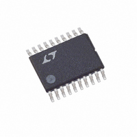
LTC3417AIFE-1#PBF Linear Technology, LTC3417AIFE-1#PBF Datasheet - Page 3

LTC3417AIFE-1#PBF
Manufacturer Part Number
LTC3417AIFE-1#PBF
Description
IC BUCK SYNC ADJ 1A/1.5A 20TSSOP
Manufacturer
Linear Technology
Type
Step-Down (Buck)r
Datasheet
1.LTC3417AEDHC-1PBF.pdf
(20 pages)
Specifications of LTC3417AIFE-1#PBF
Internal Switch(s)
Yes
Synchronous Rectifier
Yes
Number Of Outputs
2
Voltage - Output
0.8 ~ 5 V
Current - Output
1A, 1.5A
Frequency - Switching
1.5MHz, 0.6MHz ~ 4MHz
Voltage - Input
2.25 ~ 5.5 V
Operating Temperature
-40°C ~ 125°C
Mounting Type
Surface Mount
Package / Case
20-TSSOP Exposed Pad, 20-eTSSOP, 20-HTSSOP
Lead Free Status / RoHS Status
Lead free / RoHS Compliant
Power - Output
-
temperature range, otherwise specifi cations are at T
SYMBOL
V
ΔV
ΔV
g
I
I
f
I
I
R
R
I
I
V
V
R
t
V
V
I
I
VTL
VTH
VTH
ELECTRICAL CHARACTERISTICS
S
S
OSC
LIM1
LIM2
SW1(LKG)
SW2(LKG)
POR
RUN1,
SYNC/MODE
m(EA)
TH(POR)
FB1
UVLO
RUN1,
PHASE
DS(ON)1
DS(ON)2
POR
LINEREG
LOADREG
SYNC/MODE
SYNC/MODE
FREQ
, V
I
FB2
V
RUN2,
RUN2
I
PHASE,
PARAMETER
Feedback Voltage
Reference Voltage Line Regulation. %/V
is the Percentage Change in V
Change in V
Output Voltage Load Regulation
Error Amplifi er Transconductance
Input DC Supply Current (Note 4)
Half Active Mode (V
Half Active Mode (V
Both Channels in Sleep Mode
Shutdown
Oscillator Frequency
Peak Switch Current Limit on SW1 (1.5A)
Peak Switch Current Limit on SW2 (1A)
SW1 Top Switch On-Resistance (1.5A)
SW1 Bottom Switch On-Resistance
SW2 Top Switch On-Resistance (1A)
SW2 Bottom Switch On-Resistance
Switch Leakage Current SW1 (1.5A)
Switch Leakage Current SW2 (1A)
Undervoltage Lockout Threshold
Power-On-Reset Threshold
Percentage Deviation of V
Steady State Value (Typically 0.8V)
Power-On-Reset Pull Down On-Resistance
Power-On-Reset De-Assertion Delay from
Fault Removal
RUN1, RUN2 Threshold
PHASE Threshold High-CMOS Levels
PHASE Threshold Low-CMOS Levels
RUN1, RUN2, PHASE and SYNC/MODE
Leakage Current
SYNC/MODE Threshold Voltage Low
SYNC/MODE Threshold Voltage High
FREQ Threshold Voltage High
Active Mode
IN
RUN2
RUN1
= 0V, 1.5A Only) V
= 0V, 1A Only)
FB
Voltage from
OUT
with a
A
= 25°C. V
CONDITIONS
(Note 3)
V
I
I
I
V
V
V
V
V
V
V
V
V
V
V
V
V
V
V
V
V
V
V
FREQ = V
FREQ Tied to GND Through 143k Resistor
V
TH1
TH1
TH1
IN
FB1
RUN1
FB1
FB2
FB1
RUN2
RUN1
FREQ
FREQ
FREQ
IN1
IN1
IN2
IN2
IN1
IN2
IN1
IN1
FB1
FB1
IN
The
= 2.25V to 5V (Note 3)
= 6V, Pin Under Test = 3V
, I
, I
, I
, V
, V
= 3.6V (Note 5)
= 3.6V (Note 5)
= 3.6V (Note 5)
= 3.6V (Note 5)
= 6V, V
= 6V, V
= V
= 0.75V, V
= 0.75V, V
= V
or V
or V
: R
: Resistor (Note 6)
TH2
TH2
TH2(PINLOAD)
= V
= V
= V
= V
IN2
IN2
l
IN
FB2
FB2
T
FB2
FB2
IN
IN
denotes the specifi cations which apply over the full operating
= 0.36V (Note 3)
= 0.84V (Note 3)
RUN2
IN
RUN2
= 143k
Ramping Down
Ramping Up
= 3.6V unless otherwise specifi ed (Note 2).
RUN1
RUN2
= 0.75V, V
= 1V, V
Ramping Up
Ramping Down
SYNC/MODE
SYNC/MODE
= V
= 0V
= 0V
= 0V
= ±5μA (Note 3)
IN
SYNCMODE
SYNC/MODE
= V
= V
= V
IN
IN
, V
, V
IN
= V
RUN1
RUN2
, V
IN
RUN1
,
= V
= V
=
IN
IN
l
V
V
V
0.784
IN
IN
IN
MIN
0.85
1.95
1.2
2.1
1.4
1.9
0.3
–0.5
–0.5
–0.5
LTC3417A-1
212,992
294,912
–0.02
0.088
0.084
±0.01
1400
0.02
0.02
0.01
0.16
0.15
0.01
0.01
2.07
2.12
0.85
TYP
400
260
260
125
120
0.8
1.5
2.5
1.7
–6
–8
1
0.816
MAX
–0.2
1.25
2.25
600
400
400
250
300
0.2
0.2
1.8
2.2
1.5
0.5
0.5
±1
1
4
1
1
3417a1fa
UNITS
Cycles
Cycles
Clock
Clock
3
MHz
MHz
MHz
%/V
μS
μA
μA
μA
μA
μA
μA
μA
μA
%
%
%
%
Ω
Ω
Ω
Ω
Ω
V
A
A
V
V
V
V
V
V
V
V


