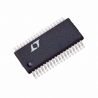
LTC3731HG Linear Technology, LTC3731HG Datasheet - Page 20

LTC3731HG
Manufacturer Part Number
LTC3731HG
Description
IC REG SW SYNC 3PH STPDWN 36SSOP
Manufacturer
Linear Technology
Series
PolyPhase®r
Type
Step-Down (Buck)r
Specifications of LTC3731HG
Internal Switch(s)
No
Synchronous Rectifier
Yes
Number Of Outputs
1
Voltage - Output
0.6 ~ 6 V
Frequency - Switching
225kHz ~ 680kHz
Voltage - Input
4 ~ 36 V
Operating Temperature
-40°C ~ 140°C
Mounting Type
Surface Mount
Package / Case
36-SSOP
Lead Free Status / RoHS Status
Contains lead / RoHS non-compliant
Current - Output
-
Power - Output
-
Lead Free Status / Rohs Status
Not Compliant
Available stocks
Company
Part Number
Manufacturer
Quantity
Price
Part Number:
LTC3731HG
Manufacturer:
LINEAR/凌特
Quantity:
20 000
Part Number:
LTC3731HG#PBF
Manufacturer:
LINEAR/凌特
Quantity:
20 000
Part Number:
LTC3731HG#TRPBF
Manufacturer:
LINEAR/凌特
Quantity:
20 000
APPLICATIO S I FOR ATIO
LTC3731H
down the PLLFLTR pin. If the external and internal fre-
quencies are the same, but exhibit a phase difference, the
current sources turn on for an amount of time correspond-
ing to the phase difference. Thus, the voltage on the
PLLFLTR pin is adjusted until the phase and frequency of
the external and internal oscillators are identical. At this
stable operating point, the phase comparator output is
open and the filter capacitor C
PLLIN pin must be driven from a low impedance source
such as a logic gate located close to the pin. When using
multiple ICs for a phase-locked system, the PLLFLTR pin
of the master oscillator should be biased at a voltage that
will guarantee the slave oscillator(s) ability to lock onto the
master’s frequency. A voltage of 1.7V or below applied to
the master oscillator’s PLLFLTR pin is recommended in
order to meet this requirement. The resultant operating
frequency will be approximately 550kHz for 1.7V.
The loop filter components (C
current pulses from the phase detector and provide a
stable input to the voltage controlled oscillator. The filter
components C
acquires lock. Typically R
0.01µF to 0.1µF.
Minimum On-Time Considerations
Minimum on-time, t
that the IC is capable of turning on the top MOSFET. It is
20
LP
and R
U
ON(MIN)
LP
U
LP
, is the smallest time duration
determine how fast the loop
=10k and C
LP
LP
holds the voltage. The IC
, R
W
PLLIN
LP
EXTERNAL
) smooth out the
OSC
LP
Figure 9. Phase-Locked Loop Block Diagram
ranges from
U
PHASE
DETECTOR/
OSCILLATOR
50k
FREQUENCY
DETECTOR
DIGITAL
PHASE/
OSC
determined by internal timing delays and the gate charge
of the top MOSFET. Low duty cycle applications may
approach this minimum on-time limit and care should be
taken to ensure that:
If the duty cycle falls below what can be accommodated by
the minimum on-time, the IC will begin to skip every other
cycle, resulting in half-frequency operation. The output
voltage will continue to be regulated, but the ripple current
and ripple voltage will increase.
The minimum on-time for the IC is generally about 110ns.
However, as the peak sense voltage decreases the mini-
mum on-time gradually increases. This is of particular
concern in forced continuous applications with low ripple
current at light loads. If the duty cycle drops below the
minimum on-time limit in this situation, a significant
amount of cycle skipping can occur with correspondingly
larger current and voltage ripple.
If an application can operate close to the minimum on-
time limit, an inductor must be chosen that is low enough
in value to provide sufficient ripple amplitude to meet the
minimum on-time requirement. As a general rule, keep
the inductor ripple current for each channel equal to or
greater than 30% of I
t
ON MIN
2.4V
(
3731H F09
)
<
V f
V
PLLFLTR
R
10k
IN
OUT
LP
( )
C
OUT(MAX)
LP
at V
IN(MAX)
.
3731hfa


