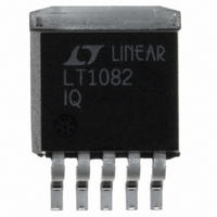
LT1082IQ#TRPBF Linear Technology, LT1082IQ#TRPBF Datasheet - Page 8

LT1082IQ#TRPBF
Manufacturer Part Number
LT1082IQ#TRPBF
Description
IC SWTCHNG REG HI-V/EFF 1A 5-DD
Manufacturer
Linear Technology
Type
Step-Down (Buck), Step-Up (Boost), Inverting, Flyback, Forward Converterr
Datasheet
1.LT1082CN8PBF.pdf
(12 pages)
Specifications of LT1082IQ#TRPBF
Internal Switch(s)
Yes
Synchronous Rectifier
No
Number Of Outputs
1
Current - Output
1A
Frequency - Switching
60kHz
Voltage - Input
3 ~ 75 V
Operating Temperature
-40°C ~ 125°C
Mounting Type
Surface Mount
Package / Case
D²Pak, TO-263 (5 leads + tab)
Power - Output
20W
Lead Free Status / RoHS Status
Lead free / RoHS Compliant
Voltage - Output
-
Available stocks
Company
Part Number
Manufacturer
Quantity
Price
OPERATIO
LT1082
disconnect the main error amplifier output and connects
the output of the flyback amplifier to the comparator input.
The LT1082 will then regulate the value of the flyback pulse
with respect to the supply voltage. This flyback pulse is
directly proportional to output voltage in the traditional
transformer coupled flyback topology regulator. By
regulating the amplitude of the flyback pulse, the output
voltage can be regulated with no direct connection between
input and output. The output is fully floating up to the
breakdown voltage of the transformer windings. Multiple
floating outputs are easily obtained with additional
windings. A special delay network inside the LT1082
ignores the leakage inductance spike at the leading edge of
the flyback pulse to improve output regulation.
When I
LT1082 shifts the switching frequency down to 12kHz.
This unique feature provides high voltage short-circuit
protection in systems like the telecom 5V supplies with
input voltages down to – 70V; lower frequency is needed
under short-circuit conditions with current mode switchers
because minimum “on” time cannot be forced below the
internally set blanking time. Referring to the telecom 5V
supply circuit on the front page, with output shorted to
ground, the V
1mA. If the FB pin is forced to source more than 1mA, the
frequency shifting function may be defeated. Therefore,
the minimum suggested value for R
maximum suggested value is 1.2k. Also, no capacitance
more than 1nF should be used on the FB pin, because it
may cause unstable switching frequency in this low
frequency mode.
The error signal developed at the comparator input is
brought out externally. This pin (V
functions. It is used for frequency compensation, current
limit adjustment, soft starting, and total regulator shutdown.
During normal regulator operation this pin sits at a voltage
between 0.9V (low output current) and 2V (high output
current). The error amplifiers are current output (g
types, so this voltage can be externally clamped for
adjusting current limit. Likewise, a capacitor-coupled
external clamp will provide soft start. Switch duty cycle
goes to zero if the V
diode, placing the LT1082 in an idle mode. Pulling the V
pin below 0.15V causes total regulator shutdown, with
8
FB
drawn out of the FB pin reaches 350 A, the
FB
U
stays at 0.6V when sourcing I
C
pin is pulled to ground through a
C
) has four different
FB
is 1k and the
FB
up to
m
C
)
only 120 A supply current for shutdown circuitry biasing.
See AN19 for full application details.
Extra Pins on the MiniDIP Packages
The miniDIP LT1082 has the emitters of the power
transistor brought out separately from the ground pin.
This eliminates errors due to ground pin voltage drops and
allows the user to reduce switch current limit by a factor
of 2:1 by leaving the second emitter (E2) disconnected.
The first emitter (E1) should always be connected to the
ground pin. Note that switch “on” resistance doubles
when E2 is left open, so efficiency will suffer somewhat
when switch currents exceed 100mA. Also, note that chip
dissipation will actually increase with E2 open during
normal load operation, even though dissipation in current
limit mode will decrease . See “Thermal Considerations.”
Thermal Considerations When Using the
MiniDIP Packages
The low supply current and high switch efficiency of the
LT1082 allow it to be used without a heat sink in most
applications when the TO-220 package is selected.
This package is rated at 50 C/W. The miniDIPs, however,
are rated at 100 C/W in ceramic (J) and 90 /W in plastic
(N).
Care should be taken for miniDIP applications to ensure
that the worst case input voltage and load current conditions
do not cause excessive die temperatures. The following
formulas can be used as a rough guide to calculate LT1082
power dissipation. For more details, the reader is referred
to Application Note 19 (AN19), “Efficiency Calculations”
section.
Average supply current (including driver current) is:
I
DC = switch duty cycle
Switch power dissipation is given by:
R
SW
SW
I
P
IN
= switch current
SW
= LT1082 switch “on” resistance (1.2 maximum)
= (I
4.5mA + I
SW
)
2
• R
SW
SW
(0.004 + DC/28)
• DC
sn1082 1082fas


