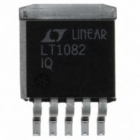
LT1082IQ#TRPBF Linear Technology, LT1082IQ#TRPBF Datasheet - Page 9

LT1082IQ#TRPBF
Manufacturer Part Number
LT1082IQ#TRPBF
Description
IC SWTCHNG REG HI-V/EFF 1A 5-DD
Manufacturer
Linear Technology
Type
Step-Down (Buck), Step-Up (Boost), Inverting, Flyback, Forward Converterr
Datasheet
1.LT1082CN8PBF.pdf
(12 pages)
Specifications of LT1082IQ#TRPBF
Internal Switch(s)
Yes
Synchronous Rectifier
No
Number Of Outputs
1
Current - Output
1A
Frequency - Switching
60kHz
Voltage - Input
3 ~ 75 V
Operating Temperature
-40°C ~ 125°C
Mounting Type
Surface Mount
Package / Case
D²Pak, TO-263 (5 leads + tab)
Power - Output
20W
Lead Free Status / RoHS Status
Lead free / RoHS Compliant
Voltage - Output
-
Available stocks
Company
Part Number
Manufacturer
Quantity
Price
OPERATIO
Total power dissipation is the sum of supply current times
input voltage plus switch power:
In a typical example, using negative-to-positive converter
to generate 5V at 0.5A from a – 45V input, duty cycle is
approximately 12%, and switch current is about 0.5A,
yielding:
Temperature rise in a plastic miniDIP would be 90 C/W
times 0.43W, or approximately 39 C. The maximum am-
bient temperature would be limited to 100 C (commercial
temperature limit) minus 39 C, or 61 C.
In most applications, full load current is used to calculate
die temperature. However, if overload conditions must
also be accounted for, four approaches are possible. First,
if loss of regulated output is acceptable under overload
conditions, the internal thermal limit of the LT1082 will
protect the die in most applications by shutting off switch
current. Thermal limit is not a tested parameter, however,
and should be considered only for noncritical applications
with temporary overloads. A second approach is to use the
larger TO-220 (T) package which, even without a heat sink,
may limit die temperatures to safe levels under overload
conditions. In critical situations, heat sinking of these
packages is required; especially if overload conditions
must be tolerated for extended periods of time.
The third approach for lower current applications is to
leave the second switch emitter (miniDIP only) open. This
increases switch “on” resistance by 2:1, but reduces
switch current limit by 2:1 also, resulting in a net 2:1
reduction in I
conditions.
The fourth approach is to clamp the V
than its internal clamp level of 2V. The LT1082 switch
current limit is zero at approximately 1V on the V
1.6A at 2V on the V
externally clamped between these two levels with a diode.
See AN19 for details.
P
I
P
P
IN
TOT
SW
TOT
= 4.5mA + 0.5(0.004 + DC/28) = 8.7mA
= (0.5)
= (I
= (45V)(8.7mA) + 0.036 = 0.43W
IN
)(V
2
2
R switch dissipation under current limit
• 1.2 • (0.12) = 0.036W
IN
U
) + P
C
SW
pin. Peak switch current can be
C
pin to a voltage less
C
pin and
LT1082 Synchronizing
The LT1082 can be externally synchronized in the fre-
quency range of 75kHz to 90kHz. This is accomplished as
shown in the accompanying figures. Synchronizing oc-
curs when the V
transistor. To avoid disturbing the DC characteristics of
the internal error amplifier, the width of the synchronizing
pulse should be under 1 s. C2 sets the pulse width at
0.6 s. The effect of a synchronizing pulse on the LT1082
amplifier offset can be calculated from:
KT/q = 26mV at 25 C
t
f
I
V
R3 = resistor used to set mid-frequency “zero” in LT1082
With t
voltage shift is 5mV. This is not particularly bothersome,
but note that high offset could result if R3 were reduced to
a much lower value. Also, the synchronizing transistor
must sink higher currents with low values of R3, so larger
drives may have to be used. The transistor must be
capable of pulling the V
ensure synchronizing.
S
S
C
C
= pulse width
= pulse frequency
= LT1082 V
= LT1082 operating V
V
frequency compensation network.
S
OS
GND
V
= 0.6 s, f
IN
LT1082
C1
KT
R3
q
C
V
source current ( 200 A)
C
C
S
Synchronizing the LT1082
pin is pulled to ground with an external
= 80kHz, V
t
S
VN2222*
f
I
C
C
S
*SILICONIX OR EQUIVALENT
pin to within 100mV of ground to
C
I
voltage (1V to 2V)
C
C
= 1.5V, and R3 = 2k, offset
R
1N4148
R2
2.2k
V
C
3
D1
D2
1N4148
350pF
C2
LT1082
FROM 5V
LOGIC
1082 OP01
sn1082 1082fas
9


