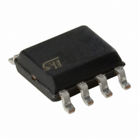
L4979D STMicroelectronics, L4979D Datasheet - Page 5

L4979D
Manufacturer Part Number
L4979D
Description
IC VOLTAGE REG LDO SO-8
Manufacturer
STMicroelectronics
Type
Step-Down (Buck)r
Specifications of L4979D
Internal Switch(s)
Yes
Synchronous Rectifier
No
Number Of Outputs
1
Voltage - Output
5V
Current - Output
150mA
Voltage - Input
5.6 ~ 31 V
Operating Temperature
-40°C ~ 150°C
Mounting Type
Surface Mount
Package / Case
8-SOIC (3.9mm Width)
Polarity
Positive
Input Voltage Max
31 V
Output Voltage
5 V
Output Type
Fixed
Dropout Voltage (max)
0.4 V at 150 mA
Output Current
300 mA
Line Regulation
25 mV
Load Regulation
25 mV
Voltage Regulation Accuracy
2 %
Maximum Operating Temperature
+ 150 C
Mounting Style
SMD/SMT
Minimum Operating Temperature
- 40 C
Lead Free Status / RoHS Status
Lead free / RoHS Compliant
Power - Output
-
Frequency - Switching
-
Lead Free Status / Rohs Status
Lead free / RoHS Compliant
Available stocks
Company
Part Number
Manufacturer
Quantity
Price
Part Number:
L4979D
Manufacturer:
ST
Quantity:
20 000
Company:
Part Number:
L4979D013TR
Manufacturer:
st
Quantity:
3 000
Part Number:
L4979D013TR
Manufacturer:
ST
Quantity:
20 000
Part Number:
L4979DTR-S-LF
Manufacturer:
ST
Quantity:
20 000
ELECTRICAL CHARACTERISTICS (continued)
Note: 1. see fig4 (behavior of output current versus regulated voltage Vo)
2
The voltage regulator uses a p-channel MOS transistor as a regulating element. With this structure a low drop-
out voltage at current up to 150mA is achieved. The output voltage is regulated up to transient input supply volt-
age of 40V. No functional interruption due to over-voltage pulses is generated. The high precision of the output
voltage is obtained with a pre-trimmed reference voltage. A short circuit protection to GND is provided.
Figure 4. Behavior of output current versus regulated voltage Vo (see a.m. Note 1)
3
The reset circuit monitors the output voltage Vo. If the output voltage drops below V
with a delay time trr. Real trr value changes as a non-linear function of delta (V
guaranteed for an output voltage Vo greater than 1V.
When the output voltage becomes higher than Vo_th then Res goes high with a delay trd. This delay is obtained
by 512 periods of an oscillator (see fig. 5). The oscillator period is given by:
ENABLE
Pin
V
V
V
R
E
E
E
E
cw
cw
cw
es
VOLTAGE REGULATOR
RESET
n
n
n
n
2. guaranteed by design
3. When Vo becomes lower than 4V, the reset reaction time decreases down to 2µs assuring a faster reset condition in this particular
case.
Symbol
V
V
I
V
T
I
I
en_hy
_leak
t
en_h
cwc
cwd
wop
wol
en_l
Charge current
Discharge current
Watchdog period
Watchdog output low time
Enable input low voltage
Enable input high voltage
Enable input hysteresis
Pull down current
Parameter
Vo_ref
Vo_ref
Vo
Vo
V
V
V
V
E
s
s
s
s
n
= 13.5V, V
= 13.5V, V
= 13.5V, C
= 13.5V, C
= 5V
Test Condition
Ishort Ilim
Ishort Ilim
cw
cw
tw
tw
= 47nF
= 47nF
= 0.1V
= 2.5V
Iout
Iout
o-th
Min.
700
1.0
25
4
6
3
2
- V
o_th
o
). The reset low signal is
1000
Typ.
then Res becomes low
7.5
2.4
50
10
10
L4979MD L4979D
Max.
1100
4.5
22
14
90
20
1
Unit
mV
ms
ms
µA
µA
µA
V
V
5/10


