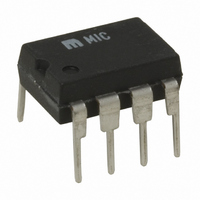
MIC3172YN Micrel Inc, MIC3172YN Datasheet - Page 11

MIC3172YN
Manufacturer Part Number
MIC3172YN
Description
IC REG SW 100KHZ 1.25A 8-DIP
Manufacturer
Micrel Inc
Type
Step-Down (Buck), Step-Up (Boost), Inverting, Cukr
Specifications of MIC3172YN
Internal Switch(s)
Yes
Synchronous Rectifier
No
Number Of Outputs
1
Current - Output
1.25A
Frequency - Switching
100kHz
Voltage - Input
3 ~ 40 V
Operating Temperature
-40°C ~ 85°C
Mounting Type
Through Hole
Package / Case
8-DIP (0.300", 7.62mm)
Power - Output
302mW
Primary Input Voltage
40V
No. Of Outputs
1
Output Current
3A
No. Of Pins
8
Operating Temperature Range
-40°C To +85°C
Supply Voltage Range
3V To 40V
Termination Type
Through Hole
Lead Free Status / RoHS Status
Lead free / RoHS Compliant
Voltage - Output
-
Lead Free Status / RoHS Status
Lead free / RoHS Compliant, Lead free / RoHS Compliant
Other names
576-2255
MIC3172YN
MIC3172YN
MIC2172/3172
Then:
The junction temperature for any semiconductor is calculated
using the following:
Where:
For the practical example:
Then:
This junction temperature is below the rated maximum of
150°C.
Grounding
Refer to figure 10. Heavy lines indicate high current paths.
A single point ground is strongly recommended for proper
operation.
The signal ground, compensation network ground, and feed-
back network connections are sensitive to minor voltage
variations. The input and output capacitor grounds and
power ground conductors will exhibit voltage drop when
carrying large currents. Keep the sensitive circuit ground
traces separate from the power ground traces. Small voltage
variations applied to the sensitive circuits can prevent the
MIC2172/3172 or any switching regulator from functioning
properly.
April 2005
P
P
P
P
T
T
T
P
θ
T
θ
T
T
V
JA
JA
J
J
A
A
J
J
SW
(SW)
(total)
(total)
(total)
IN
= T
= junction temperature
= 70 + 0.30 × 130
= 109°C
= ambient temperature (maximum)
= 70°C
= junction to ambient thermal resistance
= 130°C/W (for plastic DIP)
= (0.625)
Figure 10. Single Point Ground
= 0.234W
A
= 0.068 + 0.234
= 0.302W
= total power dissipation
* MIC3172 only
+ P
(total)
EN
P1 P2 S
MIC2172/3172
GND
2
*
× 1 × 0.6
θ
V
JA
IN
V
V
C
FB
SW
Single point ground
11
Applications and Design Hints
Access to both the collector and emitter(s) of the NPN power
switch makes the MIC2172/3172 extremely versatile and
suitable for use in most PWM power supply topologies.
Boost Conversion
Refer to figure 11 for a typical boost conversion application
where a +5V logic supply is available but +12V at 0.14A is
required.
The first step in designing a boost converter is determining
whether inductor L1 will cause the converter to operate in
either continuous or discontinuous mode. Discontinuous
mode is preferred because the feedback control of the
converter is simpler.
When L1 discharges its current completely during the
MIC2172/3172’s off-time, it is operating in discontinuous
mode.
L1 is operating in continuous mode if it does not discharge
completely before the MIC2172/3172 power switch is turned
on again.
Discontinuous Mode Design
Given the maximum output current, solve equation (1) to
determine whether the device can operate in discontinuous
mode without initiating the internal device current limit.
(1)
(1a)
Where:
I
I
V
δ = duty cycle
I
δ =
CL
OUT
OUT
N/C
IN
R3
1k
* Locate near MIC2172 when supply leads > 2"
Figure 11. 5V to 12V Boost Converter
(4.75V min.)
= internal switch current limit
= minimum input voltage
V
= maximum output current
+5V
I
I
(Refer to Electrical Characteristics.)
OUT
≤
C3
1µF
CL
CL
COMP
SYNC
V
= 1.25A when δ < 50%
= 0.833 (2 – δ) when δ ≥ 50%
OUT
P1 P2
I
+ V
MIC2172
CL
2
GND
V
V
V
+ V
OUT
F
IN
± V
S
F
IN
V
FB
27µH
SW
IN
δ
L1
1N5822
D1
C1*
22µF
C2
470µF
+12V, 0.14A
R1
10.7k
1%
R2
1.24k
1%
V
OUT
M9999-042205
Micrel, Inc.


