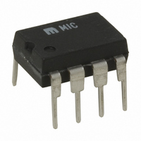
MIC3172YN Micrel Inc, MIC3172YN Datasheet - Page 12

MIC3172YN
Manufacturer Part Number
MIC3172YN
Description
IC REG SW 100KHZ 1.25A 8-DIP
Manufacturer
Micrel Inc
Type
Step-Down (Buck), Step-Up (Boost), Inverting, Cukr
Specifications of MIC3172YN
Internal Switch(s)
Yes
Synchronous Rectifier
No
Number Of Outputs
1
Current - Output
1.25A
Frequency - Switching
100kHz
Voltage - Input
3 ~ 40 V
Operating Temperature
-40°C ~ 85°C
Mounting Type
Through Hole
Package / Case
8-DIP (0.300", 7.62mm)
Power - Output
302mW
Primary Input Voltage
40V
No. Of Outputs
1
Output Current
3A
No. Of Pins
8
Operating Temperature Range
-40°C To +85°C
Supply Voltage Range
3V To 40V
Termination Type
Through Hole
Lead Free Status / RoHS Status
Lead free / RoHS Compliant
Voltage - Output
-
Lead Free Status / RoHS Status
Lead free / RoHS Compliant, Lead free / RoHS Compliant
Other names
576-2255
MIC3172YN
MIC3172YN
MIC2172/3172
For the example in figure 11.
Then:
This value is greater than the 0.14A output current require-
ment so we can proceed to find the inductance value of L1.
(2)
Where:
For our practical example:
Equation (3) solves for L1’s maximum current value.
(3)
Where:
Use a 27µH inductor with a peak current rating of at least
1.4A.
Flyback Conversion
Flyback converter topology may be used in low power appli-
cations where voltage isolation is required or whenever the
input voltage can be less than or greater than the output
voltage. As with the step-up converter the inductor (trans-
former primary) current can be continuous or discontinuous.
Discontinuous operation is recommended.
Figure 12 shows a practical flyback converter design using
the MIC3172.
M9999-042205
V
V
I
I
V
δ = 0.623
V
V
I
P
f
I
T
I
I
I
I
L1 ≤
L1 ≤
OUT
CL
OUT
SW
L1
L1(peak)
L1(peak)
L1(peak)
OUT
ON
OUT
F
IN
OUT
F
OUT
= D1 forward voltage drop
= 0.6V
≤ 26.062µH (use 27µH)
= 1.147A
= 4.75V (minimum)
= 1×10
= δ / f
= 0.14A
≤ 0.141A
= required output voltage
= 12.0V
= 12 × 0.14 = 1.68W
≤
2 P
2 × 1.68 × 1× 10
(
= 1.096A
(
4.75 × 0.623
=
=
V
SW
1.147
OUT
IN
5
Hz (100kHz)
V
4.75 × 6.23 × 10
2
δ
IN
= 6.23×10
)
f
L1
SW
× 4.75 × 0.623
2
T
27 × 10
ON
12
)
2
-6
-6
5
sec
-6
12
Switch Operation
During Q1’s on time (Q1 is the internal NPN transistor—see
block diagrams), energy is stored in T1’s primary inductance.
During Q1’s off time, stored energy is partially discharged into
C4 (output filter capacitor). Careful selection of a low ESR
capacitor for C4 may provide satisfactory output ripple volt-
age making additional filter stages unnecessary.
C1 (input capacitor) may be reduced or eliminated if the
MIC3172 is located near a low impedance voltage source.
Output Diode
The output diode allows T1 to store energy in its primary
inductance (D2 nonconducting) and release energy into C4
(D2 conducting). The low forward voltage drop of a Schottky
diode minimizes power loss in D2.
Frequency Compensation
A simple frequency compensation network consisting of R3
and C2 prevents output oscillations.
High impedance output stages (transconductance type) in
the MIC2172/3172 often permit simplified loop-stability solu-
tions to be connected to circuit ground, although a more
conventional technique of connecting the components from
the error amplifier output to its inverting input is also possible.
Voltage Clipper
Care must be taken to minimize T1’s leakage inductance,
otherwise it may be necessary to incorporate the voltage
clipper consisting of D1, R4, and C3 to avoid second break-
down (failure) of the MIC3172’s power NPN Q1.
Enable/Shutdown
The MIC3172 includes the enable/shutdown feature. When
the device is shutdown, total supply current is less than 1µA.
This is ideal for battery applications where portions of a
system are powered only when needed. If this feature is not
required, simply connect EN to V
Discontinuous Mode Design
When designing a discontinuous flyback converter, first de-
termine whether the device can safely handle the peak
primary current demand placed on it by the output power.
Equation (8) finds the maximum duty cycle required for a
given input voltage and output power. If the duty cycle is
greater than 0.8, discontinuous operation cannot be used.
(8)
For a practical example let:
P
V
I
δ ≥
CL
OUT
IN
= 1.25A when δ < 50%
= 4.0V to 6.0V
I
0.833 (2 – δ) when δ ≥ 50%
= 5.0V × 0.25A = 1.25W
CL
2 P
V
IN(min)
OUT
IN
or to a TTL high voltage.
Micrel, Inc.
April 2005


