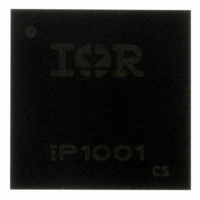
IP1001 International Rectifier, IP1001 Datasheet

IP1001
Specifications of IP1001
Available stocks
Related parts for IP1001
IP1001 Summary of contents
Page 1
... Very small outline 14mm x 14mm x 3mm Description The iP1001 is a fully optimized solution for high current synchronous buck applications requiring up to 20A. The iP1001 is optimized for single-phase applications, and includes a full function fast transient response PWM control, with an optimized power semiconductor chip-set and associated passives, achieving benchmark power density. Very few external components are required, including output inductor, input & ...
Page 2
... All specifications @ 25°C (unless otherwise specified) Absolute Maximum Ratings Parameter Symbol V to PGND PGND D0-D4 PGOOD to PGND ENABLE to PGND ILIM FREQ Output RMS Current Block Temperature Recommended Operating Conditions Parameter Symbol Supply Voltage Input Voltage Range 1 Output RMS Current from V ...
Page 3
... See Fig. 5 for Recommended Operating Area www.irf.com Min Typ Max VDD I - 600 QVDD QVIN - 300 supply outside of DAC settable range. See Design Guidelines on how to set OUT iP1001 Conditions Units - mA Enable High, 300kHz µA - Shutdown mode 1 mA Enable Low, VIN = 12V - kΩ Measured ILIM pin to SGND 3 ...
Page 4
... V = 12V 4 1.3V OUT 3.5 T =125°C BLK f set to 300kHZ 3.0 sw 2.5 2.0 1.5 1.0 0.5 0 Output Current (A) Fig 1. Power Loss vs Current Adjusting the Power Loss and SOA curves for different operating conditions To make adjustments to the power loss curves in Fig. 1, multiply the normalized value obtained from the curves in Figs the value indicated on the power loss curve in Fig ...
Page 5
... 0.91 -2 0. 0.83 3 Fig 4. Normalized Power Loss vs V OUT For 200kHz frequency setting there will be a 10% power loss reduction and a positive PCB temperature adjustment of 3°C. 3.0 3.3 iP1001 0 = 1.3V 1 OUT = 20A set to 300kHz 2 = 125°C BLK Input Voltage (V) ...
Page 6
... Shutdown : Upon receipt of the shutdown code (per VID code table above), both FETs are turned OFF and the output is discharged as the undervoltage protection is activated. 900 800 700 600 500 400 300 200 100 0 6 Fig 6. Overcurrent adjustment settings using Table 1. VID Code Table2 ...
Page 7
... conn ect code settin inputs. Internally pulled high. C urrent lim it thresh old setting pin. See ILIM curve for extern al resistor values. Switch in g frequen cy selector pin. Floating selects 300kHz, tied to V selects 200kHz Table 2. Pin Description iP1001 7 ...
Page 8
... Average VDD Current A Average VDD DC V Voltage PGOOD iP1001 FREQ ENABLE ILIM Average OUT Input P Current LOSS A Average Input DC V Voltage VO VOS VSW Averaging Circuit Average Output V Voltage VF VFS GNDS Fig 7. Power loss test circuit = V Average x I Average Average x I Average ...
Page 9
... SGND FREQ GNDS PGOOD ENABLE Fig 8. Recommended PCB Footprint (Top View) www.irf.com NC ILIM PGND iP1001 PGND 9 ...
Page 10
... User’s Design Guidelines The iP1001 is a 20A power block that consists of optimized power semiconductors, PWM control and its associated passive components based on a synchronous buck topology and offers an optimized solution where space, efficiency and noise caused by stray parasitics are of concern. The iP1001 com- ...
Page 11
... I is the output inductor ripple current. L The inductor value should be selected from 0 2.0 H range. Output Capacitor Selection Use tantalum or POSCAP type capacitors for iP1001. Selection of the output capacitors depends on several factors. • Low effective ESR for ripple and load transient requirements. ...
Page 12
... For duty cycles >50%, add external compensation ramp from the Vsw terminal of the iP1001 device as shown in the reference design through R9 resistor and C21 capacitor (Fig 10a.). For optimum perfor- mance maintain a RC time constant of approximately 5 s ...
Page 13
... The two PGND pads of the iP1001 also need to be connected to the same ground plane through vias not connect SGND pins of the iP1001 to PGND increase power supply noise immunity, place input and output capacitors close to one another, as shown in the layout diagram ...
Page 14
... This will provide 5V V necessary for the DD iP1001 internal logic to function. The boost circuit will convert 3.3V input voltage to 5V, to power the V , and will provide enough power to supply the DD internal logic for up to five iP1001 power blocks nominal IN through R2 ...
Page 15
... 1.06uH VSW C11 C12 470uF 470uF 470uF 6.3V 6.3V R3 iP1001 VFS GNDS TP2 iP1001 TP4 VOS R1 VOUT 0 C13 C14 D1 C16 470uF 0.1µF 10MQ040N 6.3V PGND PGND TP5 5-12V VIN C10 10uF 10uF ...
Page 16
... IRDCiP1001-A (For operation <4.5V Designator Value C1, C3, C5 100uF C2, C4, C6, C7, C8, C9, C10, C15 - C11, C12, C13, C14 470uF Capacitor, 6.3V, 20%, Tantalum C16, C19 0.100uF C17, C18 10.0uF C20 1.00uF C21 47.0pF D1 40V JP1, JP2, JP3 - JP1-1, JP2-1, JP3 1.06uH L2 22uH ...
Page 17
... SIDE VIEW Mechanical Drawing iP1001 NOTES: 1. DIMENSIONING & TOLERANCING PER ASME Y14.5M-1994. 2. DIMENSIONS ARE SHOWN IN MILLIMETERS [INCHES]. 3. CONTROLLING DIMENSION: MILLIMETER 4. SOLDER BALL POSITION DESIGNATION PER JESD 95-1, SPP-010. 5 PRIMARY DATUM C (SEATING PLANE) IS DEFINED BY THE SPHERICAL CROWNS OF THE SOLDER BALLS ...
Page 18
... NOTES: 1. OUTLINE CONFORMS TO EIA-481 & EIA-541. IR WORLD HEADQUARTERS: 233 Kansas St., El Segundo, California 90245, USA Tel: (310) 252-7105 18 0123 XXXX iP1001 TOP Part Marking 24mm FEED DIRECTION Tape & Reel Information Data and specifications subject to change without notice. This product has been designed and qualified for the industrial market. ...


