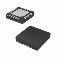
EL7520ILZ-T13 Intersil, EL7520ILZ-T13 Datasheet - Page 14

EL7520ILZ-T13
Manufacturer Part Number
EL7520ILZ-T13
Description
IC CTRLR DC/DC 4-CHAN 20-QFN
Manufacturer
Intersil
Type
Step-Up (Boost)r
Datasheet
1.EL7520AILZ-T13.pdf
(18 pages)
Specifications of EL7520ILZ-T13
Internal Switch(s)
No
Synchronous Rectifier
No
Number Of Outputs
4
Current - Output
40mA
Frequency - Switching
1MHz
Voltage - Input
3 ~ 5.5 V
Operating Temperature
-40°C ~ 85°C
Mounting Type
Surface Mount
Package / Case
20-VQFN Exposed Pad, 20-HVQFN, 20-SQFN, 20-DHVQFN
Lead Free Status / RoHS Status
Lead free / RoHS Compliant
Voltage - Output
-
Power - Output
-
under the low dropout condition (forced beta of 10). Typical
V
+1.3V to V
monitoring the output voltage. The undervoltage threshold is
set at 25% below the 1.2V reference.
Set-Up LDOs Output Voltage
Refer to Typical Application Diagram, the output voltages of
V
equations:
V
V
V
Where V
Charge Pump
To generate an output voltage higher than V
multi stages of charge pumps are needed. The number of
stage is determined by the input and output voltage. For
positive charge pump stages:
N
where V
the linear regulator. It ranges from 0.3V to 1V depending on
the transistor. V
rectifier diode.
The number of negative charge pump stages is given by:
N
To achieve high efficiency and low material cost, the lowest
number of charge pump stages, which can meet the above
requirements, is always preferred.
Charge Pump Output Capacitors
A ceramic capacitor with low ESR is recommended. With
ceramic capacitors, the output ripple voltage is dominated by
the capacitance value. The capacitance value can be
chosen by the following equation:
C
Where f
LOGIC
ON
OFF
LOGIC
ON
POSITIVE
NEGATIVE
OUT
, V
=
≥
=
OFF
V
------------------------------------------------------
2
SOC
voltage supported by EL7520, EL7520A range from
V
CE
=
REF
REF
×
REFN
DD
V
V
, and V
≥
is the dropout voltage of the pass component of
≥
REF
RIPPLE
V
------------------------------------------------------------- -
is the switching frequency.
×
-0.2V. A fault comparator is also included for
= 1.2V, V
------------------------------------------------ -
V
OUT
V
I
OUT
+
OUTPUT
1
V
F
INPUT
×
R
--------- -
R
INPUT
+
is the forward-voltage of the charge pump
LOGIC
22
21
+
R
--------- -
R
1
×
V
12
11
+
×
f
CE
–
OSC
R
--------- -
R
REFN
(
–
2
V
42
41
+
–
2
REFN
×
are determined by the following
V
V
×
V
CE
INPUT
V
F
= 0.2V.
14
F
–
V
REF
)
BOOST
, single or
EL7520, EL7520A
Start-Up Sequence
Figures 30 and 31 show detailed start-up sequence
waveforms, EL7520 and EL7520A, respectively. For a
successful power-up, there should be six peaks at V
When a fault is detected, the device will latch off until either
EN is toggled or the input supply is recycled.
If EN is L, the device is powered down. If EN is H, and the
input voltage (V
starts to charge C
ramp followed by a slow ramp. If EN is low at this point, the
C
The first four ramps on C
initialize the fault protection switch and to check whether
there is a fault condition on C
detected, the outputs and the input protection will turn off and
the chip will power down. For EL7520A, V
If no fault is found, C
until the sequence is completed.
During the second ramp, the device checks the status of
V
PG output goes low and enables the input protection PMOS
Q1. Q1 is a controlled FET used to prevent in-rush current into
V
on is controlled by C
off and disconnect the inductor from V
With the input protection FET on, NODE1 (See Typical
Application Diagram) will rise to ~V
enabled so V
diode. Hence, there is a step at V
start-up sequence. If this step is not desirable, an external
PMOS FET can be used to delay the output until the boost is
enabled internally. The delayed output appears at A
For EL7520, V
of the third ramp. The soft-start ramp depends on the value
of the C
is ~2ms. EL7520A is the same as EL7520 except that V
and V
V
peak, DELB gate goes low to turn on the external PMOS Q4
to generate a delayed V
V
PG, V
REF
BOOST
OFF
ON
DLY
is enabled at the beginning of the sixth ramp. A
OFF
LOGIC
ramp will be delayed until EN goes high.
and over temperature. At the peak of the second ramp,
turns on at the start of the fourth peak. At the fifth
DLY
before V
, DELB and V
capacitor. For C
BOOST
turn on once input voltage exceeds 2.5V.
BOOST
DD
BOOST
DLY
) exceeds 2.5V, an internal current source
o
rises to V
CDLY
. When a fault is detected, Q1 will turn
and V
to an upper threshold using a fast
ON
BOOST
DLY
is enabled internally. Its rate of turn
continues ramping up and down
are checked at end of this ramp.
LOGIC
DLY
(two up, two down) are used to
DLY
IN
-V
output.
BOOST
of 220nF, the soft-start time
or V
DIODE
IN
soft-start at the beginning
. Initially the boost is not
IN
REF
.
during this part of the
REF
through the output
. If a fault is
will stay on.
VDD
July 12, 2005
CDLY
VDD
FN7318.0
.
REF
,
.


