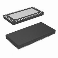
ISL65426HRZS2698 Intersil, ISL65426HRZS2698 Datasheet - Page 20

ISL65426HRZS2698
Manufacturer Part Number
ISL65426HRZS2698
Description
IC REG DUAL SYNC BUCK 6A 50-QFN
Manufacturer
Intersil
Type
Step-Down (Buck)r
Datasheet
1.ISL65426HRZ.pdf
(22 pages)
Specifications of ISL65426HRZS2698
Internal Switch(s)
Yes
Synchronous Rectifier
Yes
Number Of Outputs
2
Voltage - Output
1 ~ 4 V
Current - Output
6A
Frequency - Switching
1MHz
Voltage - Input
3 ~ 5.5 V
Operating Temperature
-10°C ~ 100°C
Mounting Type
Surface Mount
Package / Case
50-VQFN
Lead Free Status / RoHS Status
Lead free / RoHS Compliant
Power - Output
-
The following multi-layer printed circuitry board layout
strategies minimize the impact of board parasitics on
converter performance and optimize the heat-dissipating
capabilities of the printed circuit board. This section
highlights some important practices which should not be
overlooked during the layout process. Figure 38 provides a
top level view of the critical components, layer utilization,
and signal routing for reference.
Component Placement
Determine the total implementation area and orient the
critical switching components first. These include the
controller, input and output capacitors, and the output
inductors. Symmetry is very important in determining how
available space is filled and depends on the power block
configuration selected. The controller must be placed
equidistant from each output stage with the LX or phase
connection distance minimized.
An output stage consists of the area reserved for the output
inductor, and input capacitors, and output capacitors for a
single channel. Place the inductor such that one pad is a
minimal distance from the associated phase connection.
Orient the inductor such that the load device is a short
distance from the other pad. Placing the input capacitors a
minimal distance from the PVIN pins prevents long distances
from adding too much trace inductance and a reduction in
capacitor performance. Locate the output capacitors
between the inductor and the load device, while keeping
them in close proximity. Care should be taken not to add
inductance through long trace lengths that could cancel the
usefulness of the low inductance components. Keeping the
components in tight proximity will help reduce parasitic
impedances once the components are routed together.
V
C
IN
BP
GND
VCC
20
FIGURE 38. PRINTED CIRCUIT BOARD POWER PLANES AND ISLANDS
ISL65426
PGND
PVIN
LX
FB
PHASE
C
IN
V
IN
ISL65426
L
OUT
Bypass capacitors, C
placed close to their respective pins. Stray trace parasitics
will reduce their effectiveness, so keep the distance between
the VCC bias supply pad and capacitor pad to a minimum.
Plane Allocation
PCB designers typically have a set number of planes
available for a converter design. Dedicate one solid layer,
(usually an internal layer underneath the component side of
the board), for a ground plane and make all critical
component ground connections with vias to this layer.
One additional solid layer is dedicated as a power plane and
broken into smaller islands of common voltage. The power
plane should support the input power and output power
nodes. Use copper filled polygons on the top and bottom
circuit layers for the phase nodes. Use the remaining printed
circuit board layers for small signal wiring and additional
power or ground islands as required.
Signal Routing
If the output stage component placement guidelines are
followed, stray inductance in the switch current path is
minimized along with good routing techniques. Great
attention should be paid to routing the PHASE plane since
high current pulses are driven through them. Stray
inductance in this high-current path induces large noise
voltages that couple into sensitive circuitry. By keeping the
PHASE plane small, the magnitude of the potential spikes is
minimized. It is important to size traces from the LX pins to
the PHASE plane as large and short as possible to reduce
their overall impedance and inductance.
C
OUT
V
OUT
VIA CONNECTION TO GROUND PLANE
THICK TRACE ON CIRCUIT PLANE LAYER
ISLAND ON POWER PLANE LAYER
ISLAND ON CIRCUIT PLANE LAYER
C
BP
HFOUT
, supply critical filtering and must be
LOAD
KEY
March 25, 2008
FN6340.3


