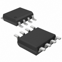
MAX850ESA+ Maxim Integrated Products, MAX850ESA+ Datasheet - Page 6

MAX850ESA+
Manufacturer Part Number
MAX850ESA+
Description
IC PWR SUP CHRG PUMP 8SOIC
Manufacturer
Maxim Integrated Products
Type
Switched Capacitor (Charge Pump), Invertingr
Datasheet
1.MAX853CSAT.pdf
(8 pages)
Specifications of MAX850ESA+
Internal Switch(s)
Yes
Synchronous Rectifier
No
Number Of Outputs
1
Voltage - Output
-4.1V, -05 ~ -9 V
Current - Output
5mA
Frequency - Switching
100kHz
Voltage - Input
4.5 ~ 10 V
Operating Temperature
-40°C ~ 85°C
Mounting Type
Surface Mount
Package / Case
8-SOIC (3.9mm Width)
Power - Output
471mW
Function
Inverting
Output Voltage
- 4.1 V or - 0.5 V to - 9 V
Output Current
5 mA
Supply Current
2 mA
Maximum Operating Temperature
+ 85 C
Input Voltage
4.5 V to 10 V
Maximum Power Dissipation
471 mW
Minimum Operating Temperature
- 40 C
Mounting Style
SMD/SMT
Switching Frequency
100 KHz
Lead Free Status / RoHS Status
Lead free / RoHS Compliant
Low-Noise, Regulated, Negative
Charge-Pump Power Supplies for GaAsFET Bias
The MAX850–MAX853 are low-noise, inverting, regulat-
ed charge-pump power supplies designed for biasing
GaAsFET devices, such as power-amplifier modules in
cellular handsets.
The applied input voltage (V
negative voltage at NEGOUT by a capacitive charge
pump. This voltage is then regulated by an internal lin-
Figure 1a. MAX850–MAX852 Block Diagram
6
______________________________________________________________Pin Description
_______________Detailed Description
MAX850
SHDN (MAX850)
SHDN (MAX851)
OSC (MAX852)
______________________________________________________________________________________
1
2
3
4
–
–
5
–
6
7
8
NEGOUT
MAX851
C1+
C1-
1
2
3
4
5
6
7
8
–
–
–
PIN
-1.28V
REF
MAX852
CHARGE
PUMP
N
1
2
3
–
–
4
5
–
6
7
8
IN
MAX853
MAX850
MAX851
MAX852
GND
) is first inverted to a
1
2
3
4
5
6
7
8
–
–
–
NEGOUT
IN
OUT
FB
NAME
CONNECT TO
GND TO SET
SHDN
SHDN
CONT
V
GND
OSC
OUT
C1+
OUT
C1-
FB
IN
= -4.1V
Positive terminal for C1
Negative terminal for C1
Negative Output Voltage (unregulated), V
Active-low TTL logic level Shutdown Input
Active-high TTL logic level Shutdown Input
External Clock Input
Dual-Mode Feedback Input. When FB is grounded, the output is preset to
-4.1V. To select other output voltages, connect FB to an external resistor
divider. See Figure 2b.
Control Voltage Input. To set V
OUT and a positive control voltage between 0V and 10V. See Figure 2c.
Output Voltage
Ground
Positive Power-Supply Input (4.5V to 10V)
ear regulator, and appears at OUT (Figure 1). The mini-
mum (most negative) output voltage (V
is the inverted positive voltage, plus the 1.0V required
by the post-regulator. The ripple noise induced by the
charge-pump inverter is reduced by the linear regulator
to 2mVp-p at V
tion, the excellent AC rejection of the linear regulator
attenuates noise on the incoming supply. Up to 5mA is
available at OUT.
Figure 1b. MAX853 Block Diagram
SHDN
NEGOUT
C1+
C1-
OUT
FUNCTION
OUT
for the MAX850–MAX852. In addi-
, connect a resistor divider between
CHARGE
PUMP
N
NEGOUT
GND
MAX853
= V
IN
OUT
+ 0.2V
IN
OUT
CONT
) achievable
CONTROL
VOLTAGE


