MAX850ESA+ Maxim Integrated Products, MAX850ESA+ Datasheet - Page 7

MAX850ESA+
Manufacturer Part Number
MAX850ESA+
Description
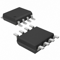
IC PWR SUP CHRG PUMP 8SOIC
Manufacturer
Maxim Integrated Products
Type
Switched Capacitor (Charge Pump), Invertingr
Datasheet
1.MAX853CSAT.pdf
(8 pages)
Specifications of MAX850ESA+
Internal Switch(s)
Yes
Synchronous Rectifier
No
Number Of Outputs
1
Voltage - Output
-4.1V, -05 ~ -9 V
Current - Output
5mA
Frequency - Switching
100kHz
Voltage - Input
4.5 ~ 10 V
Operating Temperature
-40°C ~ 85°C
Mounting Type
Surface Mount
Package / Case
8-SOIC (3.9mm Width)
Power - Output
471mW
Function
Inverting
Output Voltage
- 4.1 V or - 0.5 V to - 9 V
Output Current
5 mA
Supply Current
2 mA
Maximum Operating Temperature
+ 85 C
Input Voltage
4.5 V to 10 V
Maximum Power Dissipation
471 mW
Minimum Operating Temperature
- 40 C
Mounting Style
SMD/SMT
Switching Frequency
100 KHz
Lead Free Status / RoHS Status
Lead free / RoHS Compliant
For the MAX850–MAX852, select either a fixed or an
adjustable output voltage. Connect FB directly to GND to
select the fixed -4.1V output (Figure 2a). To select an alter-
nate output voltage, connect FB to the midpoint of a resis-
tor voltage divider from OUT to GND (Figure 2b). V
be 1.0V above the absolute value of V
regulation. The output voltage is calculated from the formu-
la below. Choose R2 to be between 100kΩ to 400kΩ.
Figure 2a. MAX850/MAX851/MAX852 Standard Application Circuit
Figure 2b. MAX850/MAX851/MAX852 Adjustable Configuration
__________Applications Information
*MAX850: SHDN
*MAX850: SHDN
Charge-Pump Power Supplies for GaAsFET Bias
MAX851: SHDN
MAX852: OSC
MAX851: SHDN
MAX852: OSC
1 F
1 F
1 F
1 F
C2
C2
C1
C1
V
OUT
_______________________________________________________________________________________
C1+
C1-
NEGOUT
SHDN*
SHDN
OSC
C1+
C1-
NEGOUT
SHDN*
SHDN
OSC
Setting the Output Voltage
= -1.28
V
MAX850
MAX851
MAX852
MAX850
MAX851
MAX852
V
IN
IN
GND
GND
IN
IN
OUT
OUT
1
FB
FB
R
R
OUT
V
2
1
OUT
Low-Noise, Regulated, Negative
= (-1.28V) 1+
to allow proper
R2
100k
R1
100k
(V
C3
1 F
C4
10 F
V
GG
OUT
of GaAsFET)
= -4.1V
(
IN
C3
1 F
C4
10 F
must
R2
R1
)
For the MAX853, set the output voltage, VOUT, by con-
necting a resistor voltage divider between OUT and a
positive control voltage, V
The MAX850–MAX853 feature a shutdown mode that
reduces the supply current to 1µA max over temperature
(5µA max for the MAX851). The MAX850 and MAX853 have
an active-low TTL logic level SHDN input, whereas the
MAX851 has an active-high SHDN input. To shut down the
MAX852, set the OCSC input to a logic-low level. The device
is powered up by the resumption of the clock signal.
Use capacitors with low effective series resistance (ESR) to
maintain a low dropout voltage (V
dropout voltage is a function of the charge pump’s output
resistance and the voltage drop across the linear regulator
(N-channel pass transistor). At the 100kHz switching fre-
quency, the charge-pump output resistance is a function of
C1 and C2’s ESR. Therefore, minimizing the ESR of the
charge-pump capacitors minimizes the dropout voltage.
1µF, 0.8Ω ESR capacitors are recommended for C1, C2,
and C3. C4 should be 10µF, 0.2Ω ESR. All capacitors
should be either surface-mount chip tantalum or chip
ceramic types. External capacitor values may be adjusted to
optimize size and cost.
Use the MAX852 to minimize system interference caused by
conflicting clock frequencies. An external oscillator can set
the charge-pump frequency and reduce clock frequency
Figure 2c. MAX853 Standard Application Circuit
1 F
1 F
C2
C1
V
OUT
C1+
C1-
NEGOUT
SHDN
= - V
Switching-Frequency Control
V
MAX853
IN
GND
IN
CTRL
CTRL
CONT
OUT
R2
R1
V
(Figure 2c.)
CTRL
IN
V
OUT
(0V TO 10V)
-
= -0.5V to -9V @ 5mA
|
V
R2
100k
R1
100k
OUT
Capacitors
|
). The overall
Shutdown
C3
1 F
C4
10 F
7


