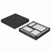
NCP3101BMNTXG ON Semiconductor, NCP3101BMNTXG Datasheet - Page 12

NCP3101BMNTXG
Manufacturer Part Number
NCP3101BMNTXG
Description
IC CONV VOLT SYNC BUCK 6A 40-QFN
Manufacturer
ON Semiconductor
Type
Step-Down (Buck)r
Datasheet
1.NCP3101BMNTXG.pdf
(26 pages)
Specifications of NCP3101BMNTXG
Internal Switch(s)
Yes
Synchronous Rectifier
Yes
Number Of Outputs
1
Voltage - Output
Adj to 0.8V
Current - Output
6A
Frequency - Switching
275kHz
Voltage - Input
4.5 ~ 13.2 V
Operating Temperature
-40°C ~ 85°C
Mounting Type
Surface Mount
Package / Case
40-TQFN Exposed Pad
Power - Output
3W
Lead Free Status / RoHS Status
Lead free / RoHS Compliant
Design Procedure
important to collect as much information as possible about
the behavior of the input and output before starting the
design.
tool available online under the design tools section of the
NCP3101C product page. The tool allows you to capture
your design point and optimize the performance of your
regulator based on your design criteria.
that are LC filtered to produce a lower DC output voltage
V
on time relative to the switching period T or switching
frequency. The ratio of high side switch on time to the
switching period is called duty ratio D. Duty ratio can also
be calculated using V
Drop V
D
F
T
T
T
V
VCC
V
V
Inductor Selection
rule of thumb for the design where the percentage of ripple
SW
OFF
ON
Table 4. DESIGN PARAMETERS
OUT
HSD
LSD
OUT
Input voltage (VCC)
Output voltage (V
Input ripple voltage (VCC
Output ripple voltage (V
Output current rating (I
Operating frequency (F
When starting the design of a buck regulator, it is
ON Semiconductor has a Microsoft Excel® based design
The buck converter produces input voltage V
When selecting an inductor, the designer may employ a
27.5% +
. The output voltage can be changed by modifying the
LSD
D +
Design Parameter
, and High Side Switch Voltage Drop V
V
3.3 V
12 V
= Duty cycle
= Switching frequency
= Switching period
= High side switch off time
= High side switch on time
= High side switch voltage drop
= Input voltage
= Low side switch voltage drop
= Output voltage
CC
D +
V
OUT
* V
OUT
)
T
OUT
OUT
HSD
SW
) V
OUTRIPPLE
T
ON
RIPPLE
F
)
)
, V
( 1 * D ) +
SW
) V
LSD
CC
+
)
LSD
, Low Side Switch Voltage
)
1
T
[ D +
T
OFF
T
10.8 V to 13.2 V
Example Value
V
V
OUT
CC
275 kHz
300 mV
40 mV
3.3 V
APPLICATION SECTION
6 A
³
CC
HSD
(eq. 2)
(eq. 3)
(eq. 4)
http://onsemi.com
pulses
.
12
current in the inductor should be between 10% and 40%.
When using ceramic output capacitors, the ripple current can
be greater because the ESR of the output capacitor is small,
thus a user might select a higher ripple current. However,
when using electrolytic capacitors, a lower ripple current
will result in lower output ripple due to the higher ESR of
electrolytic capacitors. The ratio of ripple current to
maximum output current is given in Equation 5.
DI
I
ra
Using the ripple current rule of thumb, the user can establish
acceptable values of inductance for a design using
Equation 6.
D
F
I
L
ra
When selecting an inductor, the designer must not exceed
the current rating of the part. To keep within the bounds of
the part’s maximum rating, a calculation of the RMS current
and peak current are required.
OUT
OUT
SW
OUT
5.6 mH +
15
13
11
L
9
7
5
3
1
OUT
10
Figure 26. Inductance vs. Current Ripple Ratio
+
13
I
6.0 A * 26% * 275 kHz
OUT
= Ripple current
= Output current
= Ripple current ratio
= Duty ratio
= Switching frequency
= Output current
= Output inductance
= Ripple current ratio
16
V
* ra * F
RIPPLE CURRENT RATIO (%)
OUT
19
12 V
13V
7V
5V
SW
ra +
22
* ( 1 * D ) ³
I
OUT
25
DI
* ( 1 * 27.5% )
28
31
5.6 mH
34
37 40
(eq. 5)
(eq. 6)


