NCP3101BMNTXG ON Semiconductor, NCP3101BMNTXG Datasheet - Page 3
NCP3101BMNTXG
Manufacturer Part Number
NCP3101BMNTXG
Description
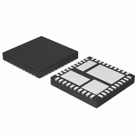
IC CONV VOLT SYNC BUCK 6A 40-QFN
Manufacturer
ON Semiconductor
Type
Step-Down (Buck)r
Datasheet
1.NCP3101BMNTXG.pdf
(26 pages)
Specifications of NCP3101BMNTXG
Internal Switch(s)
Yes
Synchronous Rectifier
Yes
Number Of Outputs
1
Voltage - Output
Adj to 0.8V
Current - Output
6A
Frequency - Switching
275kHz
Voltage - Input
4.5 ~ 13.2 V
Operating Temperature
-40°C ~ 85°C
Mounting Type
Surface Mount
Package / Case
40-TQFN Exposed Pad
Power - Output
3W
Lead Free Status / RoHS Status
Lead free / RoHS Compliant


Table 1. PIN FUNCTION DESCRIPTION
Table 2. ABSOLUTE MAXIMUM RATINGS
Main Supply Voltage Control Input
Main Supply Voltage Power Input
Bootstrap Supply Voltage vs Ground
Bootstrap Supply Voltage vs Ground (spikes < =
50 ns)
14,15,19,20,23
1−4, 36−40
Pin No
26−34
5−12
13
16
17
18
21
22
24
25
35
Pin Name
COMP/DIS
PWRGND
PWRPHS
PWRVCC
Symbol
TGOUT
AGND
CPHS
TGIN
VCC
BST
NC
BG
FB
PWRGND 5
PWRGND 6
PWRGND 7
PWRGND 8
PWRGND 9
PWRGND 10
PWRPHS 1
PWRPHS 2
PWRPHS 3
PWRPHS 4
Power phase node (PWRPHS). Drain of the low side power MOSFET.
Power ground. High current return for the low−side power MOSFET. Connect
PWRGND with large copper areas to the input and output supply returns, and
negative terminals of the input and output capacitors.
Supply rail for the internal circuitry. Operating supply range is 4.5 V to 13.2 V.
Decouple with a 1 mF capacitor to GND. Ensure that this decoupling capacitor is
placed near the IC.
IC ground reference. All control circuits are referenced to these pins.
The inverting input pin to the error amplifier. Use this pin in conjunction with the
COMP pin to compensate the voltage−control feedback loop. Connect this pin to the
output resistor divider (if used) or directly to output voltage.
Compensation or disable pin. The output of the error amplifier (EA) and the
non−inverting input of the PWM comparator. Use this pin in conjunction with the FB
pin to compensate the voltage−control feedback loop. The compensation capacitor
also acts as a soft start capacitor. Pull the pin below 400 mV to disable controller.
Not Connected. The pin can be connected to AGND or not connected.
High side MOSFET driver output.
The controller phase sensing for short circuit protection.
Supply rail for the floating top gate driver. To form a boost circuit, use an external
diode to bring the desired input voltage to this pin (cathode connected to BST pin).
Connect a capacitor (C
High side MOSFET gate.
Input supply pin for the high side MOSFET. Connect VCCPWR to the VCC pin or
power separately for split rail application..
The current limit set pin.
Figure 4. Pin Connections
http://onsemi.com
PWRPHS
V
PWRVCC
Symbol
BST_spike
V
V
BST
3
CC
AGND
PWRVCC
BST
) between this pin and the CPHS pin.
30 PWRVCC
29 PWRVCC
28 PWRVCC
27 PWRVCC
26 PWRVCC
25 TGIN
24 BST
23 AGND
22 CPHS
21 TGOUT
−0.3
−0.3
−0.3
−5.0
Min
Description
Max
15
30
35
40
Unit
V
V
V
V
Related parts for NCP3101BMNTXG
Image
Part Number
Description
Manufacturer
Datasheet
Request
R

Part Number:
Description:
Wide Input Voltage Synchronous Buck Converter
Manufacturer:
ON Semiconductor
Datasheet:
Part Number:
Description:
ON Semiconductor [VOLTAGE REGULATOR]
Manufacturer:
ON Semiconductor
Datasheet:
Part Number:
Description:
357-036-542-201 CARDEDGE 36POS DL .156 BLK LOPRO
Manufacturer:
ON Semiconductor
Datasheet:
Part Number:
Description:
357-036-542-201 CARDEDGE 36POS DL .156 BLK LOPRO
Manufacturer:
ON Semiconductor
Datasheet:
Part Number:
Description:
357-036-542-201 CARDEDGE 36POS DL .156 BLK LOPRO
Manufacturer:
ON Semiconductor
Datasheet:
Part Number:
Description:
357-036-542-201 CARDEDGE 36POS DL .156 BLK LOPRO
Manufacturer:
ON Semiconductor
Datasheet:
Part Number:
Description:
357-036-542-201 CARDEDGE 36POS DL .156 BLK LOPRO
Manufacturer:
ON Semiconductor
Datasheet:
Part Number:
Description:
357-036-542-201 CARDEDGE 36POS DL .156 BLK LOPRO
Manufacturer:
ON Semiconductor
Datasheet:
Part Number:
Description:
357-036-542-201 CARDEDGE 36POS DL .156 BLK LOPRO
Manufacturer:
ON Semiconductor
Datasheet:
Part Number:
Description:
357-036-542-201 CARDEDGE 36POS DL .156 BLK LOPRO
Manufacturer:
ON Semiconductor
Datasheet:
Part Number:
Description:
357-036-542-201 CARDEDGE 36POS DL .156 BLK LOPRO
Manufacturer:
ON Semiconductor
Datasheet:
Part Number:
Description:
357-036-542-201 CARDEDGE 36POS DL .156 BLK LOPRO
Manufacturer:
ON Semiconductor
Datasheet:
Part Number:
Description:
Manufacturer:
ON Semiconductor
Datasheet:
Part Number:
Description:
Manufacturer:
ON Semiconductor
Datasheet: