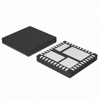
NCP3101BMNTXG ON Semiconductor, NCP3101BMNTXG Datasheet - Page 16

NCP3101BMNTXG
Manufacturer Part Number
NCP3101BMNTXG
Description
IC CONV VOLT SYNC BUCK 6A 40-QFN
Manufacturer
ON Semiconductor
Type
Step-Down (Buck)r
Datasheet
1.NCP3101BMNTXG.pdf
(26 pages)
Specifications of NCP3101BMNTXG
Internal Switch(s)
Yes
Synchronous Rectifier
Yes
Number Of Outputs
1
Voltage - Output
Adj to 0.8V
Current - Output
6A
Frequency - Switching
275kHz
Voltage - Input
4.5 ~ 13.2 V
Operating Temperature
-40°C ~ 85°C
Mounting Type
Surface Mount
Package / Case
40-TQFN Exposed Pad
Power - Output
3W
Lead Free Status / RoHS Status
Lead free / RoHS Compliant
P
are the losses associated with turning the high−side
MOSFET on and off and the corresponding overlap in drain
voltage and current.
P
F
I
P
P
P
t
t
VCC
side MOSFET it is important to know the charge
characteristic shown in Figure 28.
I
Q
R
R
t
V
V
I
Q
FALL
RISE
RISE
OUT
G1
G2
SW_TOT
SW
SW
SW
TON
TOFF
t
GD
HSPU
G
BST
TH
t
GD
The first term for total switching losses from Equation 24
When calculating the rise time and fall time of the high
Figure 28. High Side MOSFET Gate−to−Source and
RISE
FALL
Vth
+ P
+
Drain−to−Source Voltage vs. Total Charge
+
+
1
2
TON
@ I
Q
Q
I
I
G1
G2
GD
GD
OUT
) P
+
+
= High side MOSFET total switching
= Switching frequency
= Load current
= High side MOSFET switching losses
= Turn on power losses
= Turn off power losses
= MOSFET fall time
= MOSFET rise time
= Input voltage
= Output current from the high−side gate
= MOSFET gate to drain gate charge
= Drive pull up resistance
= MOSFET gate resistance
= MOSFET rise time
= Boost voltage
= MOSFET gate threshold voltage
= Output current from the low−side gate
= MOSFET gate to drain gate charge
@ V
TOFF
V
V
losses
drive
drive
BST
IN
BST
@ F
* V
* V
SW
TH
TH
@ t
Q
Q
GD
GD
RISE
R
R
HSPU
HSPD
) t
FALL
) R
) R
G
G
(eq. 25)
(eq. 26)
(eq. 27)
http://onsemi.com
16
R
R
t
V
V
by both the high−side and low−side MOSFETs, but are
dissipated only in the high−side MOSFET.
C
F
P
VCC
body diode in the low−side MOSFET is shown as follows:
F
P
Q
V
voltages so switching losses are negligible. The low−side
MOSFET’s power dissipation only consists of conduction
loss due to R
periods.
P
P
P
Conduction loss in the low−side MOSFET is described as
follows:
I
R
P
D
I
I
ra
The body diode losses can be approximated as:
F
I
NOL
NOL
FALL
RMS_LS
OUT
RMS_LS
OUT
SW
DS
SW
RR
BODY
COND
D_LS
COND
SW
G
HSPD
OSS
DS(ON)_LS
P
BST
TH
RR
CC
Next, the MOSFET output capacitance losses are caused
Finally, the loss due to the reverse recovery time of the
The low−side MOSFET turns on into small negative
BODY
HL
LH
+ V
I
RMS_LS
DS(on)
P
FD
= MOSFET output capacitance at 0 V
= Switching frequency
= MOSFET drain to source charge losses
= Input voltage
= Switching frequency
= High side MOSFET reverse recovery losses
= Reverse recovery charge
= Input voltage
= Low side MOSFET body diode losses
= Low side MOSFET conduction losses
= Low side MOSFET losses
COND
= RMS current in the low side
= Low−side MOSFET on resistance
= High side MOSFET conduction losses
= Duty ratio
= Load current
= RMS current in the low side
= Ripple current ratio
= Dead time between the high−side
= Dead time between the low−side
P
= Switching frequency
= Load current
@ I
DS
= MOSFET gate resistance
= Drive pull down resistance
= MOSFET fall time
= Boost voltage
= MOSFET gate threshold voltage
P
MOSFET turning off and the low−side
MOSFET turning on, typically 46 ns
P
+ I
D_LS
OUT
+
RR
and body diode loss during non−overlap
+ I
OUT
1
2
+ Q
@ F
+ P
@ C
RMS_LS
SW
@
RR
OSS
COND
@ NOL
@ V
1 * D @ 1 )
@ V
2
IN
) P
@ R
IN
@ F
LH
2
BODY
DS(on)_LS
@ F
SW
) NOL
SW
ra
12
HL
2
(eq. 28)
(eq. 29)
(eq. 30)
(eq. 31)
(eq. 32)
(eq. 33)


