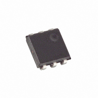
DS2401P+T&R Maxim Integrated Products, DS2401P+T&R Datasheet

DS2401P+T&R
Specifications of DS2401P+T&R
Related parts for DS2401P+T&R
DS2401P+T&R Summary of contents
Page 1
FEATURES Upgrade and drop-in replacement for DS2400 — Extended 2.8 to 6.0 voltage range — Multiple DS2401s can reside on a ® common 1-Wire Net Unique, factory-lasered and tested 64-bit registration number (8-bit family code + 48- bit serial ...
Page 2
ORDERING INFORMATION Standard Lead-Free DS2401 DS2401+ DS2401/T&R DS2401+T&R DS2401/T&R/SL DS2401-SL+T&R TO-92 Package with Straight Leads, Tape-and-Reel DS2401Z DS2401Z+ DS2401Z/T&R DS2401Z+T&R DS2401P DS2401P+ DS2401P/T&R DS2401P+T&R DS2401X1 — DESCRIPTION The DS2401 enhanced Silicon Serial Number is a low-cost, electronic registration number that ...
Page 3
DS2401 MEMORY MAP Figure 1 8-Bit CRC Code MSB LSB MSB DS2401 EQUIVALENT CIRCUIT Figure 2 BUS MASTER CIRCUIT Figure 3 Note: Depending on the 1-Wire communication speed and the bus load characteristics, the optimal pullup ) value will be ...
Page 4
TRANSACTION SEQUENCE The sequence for accessing the DS2401 via the 1-Wire port is as follows: Initialization ROM Function Command Read Data INITIALIZATION All transactions on the 1-Wire bus begin with an initialization sequence. The initialization sequence consists of a reset ...
Page 5
SIGNALING The DS2401 requires a strict protocol to ensure data integrity. The protocol consists of four types of signaling on one line: reset sequence with Reset Pulse and Presence Pulse, write 0, write 1, and read data. All these ...
Page 6
ROM FUNCTIONS FLOW CHART Figure ...
Page 7
INITIALIZATION PROCEDURE “RESET AND PRESENCE PULSES” Figure 5 RESISTOR MASTER DS2401 ∗ In order not to mask interrupt signaling by other devices on the 1-Wire bus less than 960 μ s. READ/WRITE TIMING DIAGRAM Figure 6 Write-One Time ...
Page 8
READ/WRITE TIMING DIAGRAM (cont’d) Figure 6 Write-zero Time Slot Read-data Time Slot RESISTOR MASTER DS2401 CRC GENERATION To validate the data transmitted from the DS2401, the bus master may generate a CRC value from the data received. ...
Page 9
ABSOLUTE MAXIMUM RATINGS* Voltage on any Pin Relative to Ground Operating Temperature Range Storage Temperature Range Soldering Temperature ∗ This is a stress rating only and functional operation of the device at these or any other conditions above those indicated ...
Page 10
NOTES: 1) All voltages are referenced to ground external pullup voltage. PUP 3) Input load is to ground additional reset or communication sequence cannot begin until the reset high time has expired. 5) Read data ...


