HD9P6409-9Z96 Intersil, HD9P6409-9Z96 Datasheet - Page 8
HD9P6409-9Z96
Manufacturer Part Number
HD9P6409-9Z96
Description
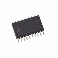
IC MED MANCHESTER 1MHZ 20-SOIC
Manufacturer
Intersil
Type
Manchester Encoder/Decoderr
Datasheet
1.HD3-6409-9Z.pdf
(14 pages)
Specifications of HD9P6409-9Z96
Applications
Security
Mounting Type
Surface Mount
Package / Case
20-SOIC (7.5mm Width)
Lead Free Status / RoHS Status
Lead free / RoHS Compliant
Available stocks
Company
Part Number
Manufacturer
Quantity
Price

Part Number:
HD9P6409-9Z96
Manufacturer:
INTERSIL
Quantity:
20 000


Absolute Maximum Ratings
Supply Voltage . . . . . . . . . . . . . . . . . . . . . . . . . . . . . . . . . . . . . +7.0V
Input, Output or I/O Voltage . . . . . . . . . . . . GND -0.5V to V
ESD Classification . . . . . . . . . . . . . . . . . . . . . . . . . . . . . . . . . Class 1
Operating Conditions
Operating Temperature Range . . . . . . . . . . . . . . . . .-40°C to +85°C
Operating Voltage Range. . . . . . . . . . . . . . . . . . . . . . +4.5V to +5.5V
Input Rise and Fall Times . . . . . . . . . . . . . . . . . . . . . . . . . 50ns Max
Sync. Transition Span (t2) . . . . . . . . . .1.5 DBP Typical, (Notes 1, 2)
Short Data Transition Span (t4) . . . . . . 0.5DBP Typical, (Notes 1, 2)
Long Data Transition Span (t5) . . . . . . 1.0DBP Typical, (Notes 1, 2)
Zero Crossing Tolerance (tCD5) . . . . . . . . . . . . . . . . . . . . . (Note 3)
CAUTION: Do not operate at or near the maximum ratings listed for extended periods of time. Exposure to such conditions may adversely impact product reliability and
result in failures not covered by warranty.
NOTES:
Common Electrical Specifications
DC Electrical Specifications
NOTES:
1. DBP-Data Bit Period, Clock Rate = 16X, one DBP = 16 Clock Cycles; Clock Rate = 32X, one DBP = 32 Clock Cycles.
2. The input conditions specified are nominal values, the actual input waveforms transition spans may vary by ±2 I
3. The maximum zero crossing tolerance is ±2 I
4. θ
5. Tested as follows: f = 16MHz, V
6. Interchanging of force and sense conditions is permitted
SYMBOL
I
X
JA
I
I
CCOP
V
V
CCSB
V
V
V
V
clock cycles (32X mode).
V
V
F
I
IHR
IHC
ILR
ILC
OH
I
I
OL
O
is measured with the component mounted on a high effective thermal conductivity test board in free air. See Tech Brief TB379 for details.
IH
IL
I
I
T
Logical “1” Input Voltage
Logical “0” Input Voltage
Logic “1” Input Voltage (Reset)
Logic “0” Input Voltage (Reset)
Logical “1” Input Voltage (Clock)
Logical “0” Input Voltage (Clock)
Input Leakage Current (Except I
Input Leakage Current (I
I/O Leakage Current
Output HIGH Voltage (All Except O
Output LOW Voltage (All Except O
Standby Power Supply Current
Operating Power Supply Current
Functional Test
PARAMETER
8
IH
= 70% V
V
CC
X
= 5.0V ± 10%, T
)
CC
X
, V
X
Parameters with MIN and/or MAX limits are 100% tested at +25°C, unless otherwise specified.
Temperature limits established by characterization and are not production tested.
clock cycles (16X mode) or ±6 I
)
IL
X
X
)
)
= 20% V
CC
A
V
V
V
V
V
V
V
V
V
I
I
V
Outputs Open
f = 16.0MHz, V
V
(Note 5)
+0.5V
= -40°C to +85°C (HD-6409-9).
OH
OL
CC
CC
CC
CC
CC
CC
IN
IN
OUT
IN
CC
CC
= +2.0mA, V
= V
= V
= V
= -2.0mA, V
HD-6409
HD-6409
= 4.5V
= 4.5V
= 5.5V
= 4.5V
= 5.5V
= 4.5V
= 5.5V, C
, V
= V
CC
CC
CC
OH
CC
TEST CONDITIONS
or GND, V
or GND, V
or GND, V
≥ V
or GND, V
L
IN
CC
= 50pF
(Note 5)
CC
CC
Thermal Information
Thermal Resistance (Typical, Note 4)
Storage Temperature Range . . . . . . . . . . . . . . . . . .-65°C to +150°C
Maximum Junction Temperature
Pb-free reflow profile . . . . . . . . . . . . . . . . . . . . . . . . . .see link below
*Pb-free PDIPs can be used for through hole wave solder
processing only. They are not intended for use in Reflow solder
processing applications.
Die Characteristics
Gate Count . . . . . . . . . . . . . . . . . . . . . . . . . . . . . . . . . . . .250 Gates
= V
/2, and V
PDIP Package . . . . . . . . . . . . . . . . . . .
SOIC Package . . . . . . . . . . . . . . . . . . .
Ceramic Package. . . . . . . . . . . . . . . . . . . . . . . . . . . . . . . . +175°C
Plastic Package . . . . . . . . . . . . . . . . . . . . . . . . . . . . . . . . . +150°C
http://www.intersil.com/pbfree/Pb-FreeReflow.asp
= 4.5V (Note 6)
= 4.5V (Note 6)
CC
X
CC
CC
CC
clock cycles (32 mode) from the nominal.
CC
or GND
= 5.5V,
= 5.5V
= 5.5V
OL
= 5.5V
≤ V
CC
/2, V
CC
70% V
V
V
V
= 4.5V and 5.5V.
CC
CC
CC
MIN
-1.0
-20
-10
-
-
-
-
-
-
-
-0.5
-0.5
-0.4
CC
X
clock cycles (16X mode) or ±6
GND +0.5
GND +0.5
20% V
θ
JA
MAX
+1.0
18.0
+20
+10
100
0.4
-
-
-
-
-
100
(°C/W)
75
CC
October 15, 2008
θ
UNITS
JC
mA
μA
μA
μA
μA
N/A
N/A
V
V
V
V
V
V
V
V
FN2951.3
-
(°C/W)
Related parts for HD9P6409-9Z96
Image
Part Number
Description
Manufacturer
Datasheet
Request
R

Part Number:
Description:
CMOS Manchester Encoder-Decoder
Manufacturer:
INTERSIL [Intersil Corporation]
Datasheet:

Part Number:
Description:
IC MED MANCHESTER 1MHZ 20-SOIC
Manufacturer:
Intersil
Datasheet:

Part Number:
Description:
Intersil Corporation [CMOS Serial Controller Interface]
Manufacturer:
Intersil Corporation
Datasheet:
Part Number:
Description:
Manufacturer:
Intersil Corporation
Datasheet:
Part Number:
Description:
357-036-542-201 CARDEDGE 36POS DL .156 BLK LOPRO
Manufacturer:
Intersil Corporation
Datasheet:
Part Number:
Description:
1024-Word x 4-Bit LSI Static RAM
Manufacturer:
Intersil Corporation
Datasheet:
Part Number:
Description:
General Purpose NPN Transistor Arrays FN341.4
Manufacturer:
Intersil Corporation
Datasheet:
Part Number:
Description:
CMOS 16-Bit Microprocessor
Manufacturer:
Intersil Corporation
Datasheet:
Part Number:
Description:
Manufacturer:
Intersil Corporation
Datasheet:
Part Number:
Description:
Manufacturer:
Intersil Corporation
Datasheet:
Part Number:
Description:
Manufacturer:
Intersil Corporation
Datasheet:
Part Number:
Description:
Manufacturer:
Intersil Corporation
Datasheet:
Part Number:
Description:
CMOS 6-Bit Latch and Decoder Memory Interfaces
Manufacturer:
Intersil Corporation
Datasheet:
Part Number:
Description:
CA3046General Purpose NPN Transistor Arrays
Manufacturer:
Intersil Corporation
Datasheet:
Part Number:
Description:
Manufacturer:
Intersil Corporation
Datasheet: