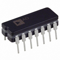
PKD01AY Analog Devices Inc, PKD01AY Datasheet

PKD01AY
Specifications of PKD01AY
Available stocks
Related parts for PKD01AY
PKD01AY Summary of contents
Page 1
GENERAL DESCRIPTION The PKD01 tracks an analog input signal until a maximum amplitude is reached. The maximum value is then retained as a peak voltage on a hold capacitor. Being a monolithic circuit, the PKD01 offers significant performance and ...
Page 2
PKD01–SPECIFICATIONS ELECTRICAL CHARACTERISTICS Parameter Symbol Conditions g AMPLIFIERS Zero-Scale Error V ZS Input Offset Voltage V OS Input Bias Current I B Input Offset Current I OS Voltage Gain A V Open-Loop Bandwidth BW Common-Mode Rejection Ratio ...
Page 3
... No Load SY ). The droop current vs. time (after power-on) curve clarifies this J ) value. ADI has a droop current cancellation circuit that minimizes droop current at high temperature. J ≤ +125 C for PKD01AY, –25 C ≤ ≤ +70 C for PKD01EP, PKD01FP, unless otherwise noted.) PKD01A/E PKD01F Min Typ ...
Page 4
... Storage Temperature Range PKD01AY, PKD01EY, PKD01FY . . . . . –65°C to +150°C PKD01EP, PKD01FP . . . . . . . . . . . . . . . –65°C to +125°C Operating Temperature Range PKD01AY . . . . . . . . . . . . . . . . . . . . . . . . –55°C to +125°C PKD01EY, PKD01FY . . . . . . . . . . . . . . . . –25°C to +85°C PKD01EP, PKD01FP . . . . . . . . . . . . . . . . . . . 0°C to 70°C Junction Temperature . . . . . . . . . . . . . . . . . –65°C to +150°C ...
Page 5
WAFER TEST LIMITS (@ Parameter “g ” AMPLIFIERS Zero-Scale Error Input Offset Voltage Input Bias Current Input Offset Current Voltage Gain Common-Mode Rejection Ratio Power Supply Rejection Ratio 1 Input Voltage Range Feedthrough Error ...
Page 6
PKD01–Typical Performance Characteristics INPUT + RANGE = V+ – +125 –55 C +25 C –2 +125 C –6 –10 V– SUPPLY –14 – SUPPLY VOLTAGE ...
Page 7
ERROR 6 2mV ERROR 4 20mV ERROR 2 0 100 1k 10k 100k 1M FREQUENCY – 100 TIME – 20 s/DIV 100 ...
Page 8
PKD01 100 – 100 1k 10k 100k 1M 10M FREQUENCY – ...
Page 9
V+ FOR IN – +125 –55 C –2 +25 C +125 C –6 –10 V– –14 – SUPPLY VOLTAGE +V AND –V – V ...
Page 10
PKD01 +125 –55 C –2 +25 C –6 +125 C –10 V– –14 – SUPPLY VOLTAGE +V AND –V – V 1.0 0.8 +125 C ...
Page 11
THEORY OF OPERATION The typical peak detector uses voltage amplifiers and a diode or an emitter follower to charge the hold capacitor, C ionally (see Figure 1). The output impedance of A plus D dynamic impedance make up ...
Page 12
PKD01 APPLICATIONS INFORMATION Optional Offset Voltage Adjustment Offset voltage is the primary zero scale error component since a variable voltage clamp limits voltage excursions at D and reduces charge injection. The PKD01 circuit gain and opera- tional mode (positive or ...
Page 13
PEAK HOLD CAPACITOR RECOMMENDATIONS The hold capacitor (C ) serves as the peak memory element H and compensating capacitor. Stable operation requires a mini- mum value of 1000 pF. Larger capacitors may be used to lower droop rate errors, but ...
Page 14
PKD01 I 1 DET OR RST CURRENT TO CONTROL MODES Typical Circuit Configurations INPUT OUTPUT TIME – 50 s/DIV INPUT OUTPUT TIME – 50 s/DIV +18V DIGITAL Q 3 GROUND V– DET/RST ...
Page 15
INPUT OUTPUT TIME – 50 s/DIV INPUT OUTPUT TIME – 50 s/DIV INPUT C PKD01 B R4 RESET VOLTAGE 1000pF DET/RST 20k 10k 1% 1% +2V INPUT 0V (GAIN = –2) –5V 8.2k 30.1k ...
Page 16
PKD01 POS/NEG PEAK DETECTOR R INPUT BIT PORT PROCESSOR 0 BIT PORT PKD01 V + POSITIVE ...
Page 17
V IN –15V +15V SW-201 A1 +15V DET/RST AMPLITUDE SELECTION LOGIC CH1 CH2 CH3 CH4 RAMP MUX-08 AMPLITUDE CH5 CH6 CH7 ...
Page 18
PKD01 OUTLINE DIMENSIONS Dimensions shown in inches and (mm). 14-Lead Plastic DIP (PDIP) (N-14) 0.795 (20.19) 0.725 (18.42 0.280 (7.11) 0.240 (6.10 0.325 (8.25) PIN 1 0.300 (7.62) 0.100 (2.54) 0.060 (1.52) BSC 0.015 (0.38) 0.210 ...


