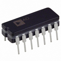
PKD01AY Analog Devices Inc, PKD01AY Datasheet - Page 13

PKD01AY
Manufacturer Part Number
PKD01AY
Description
IC MONO PEAK DETECTOR R&H 14CDIP
Manufacturer
Analog Devices Inc
Datasheet
1.PKD01FP.pdf
(18 pages)
Specifications of PKD01AY
Rohs Status
RoHS non-compliant
Applications
*
Mounting Type
Through Hole
Package / Case
14-CDIP (0.300", 7.62mm)
Power Supply Requirement
Dual
Single Supply Voltage (typ)
Not RequiredV
Single Supply Voltage (min)
Not RequiredV
Single Supply Voltage (max)
Not RequiredV
Mounting
Through Hole
Pin Count
14
Lead Free Status / RoHS Status
Not Compliant
Available stocks
Company
Part Number
Manufacturer
Quantity
Price
Company:
Part Number:
PKD01AY
Manufacturer:
SANKEN
Quantity:
310
PEAK HOLD CAPACITOR RECOMMENDATIONS
The hold capacitor (C
and compensating capacitor. Stable operation requires a mini-
mum value of 1000 pF. Larger capacitors may be used to lower
droop rate errors, but acquisition time will increase.
Zero scale error is internally trimmed for C
C
mated with the following equation.
The peak hold capacitor should have very high insulation resis-
tance and low dielectric absorption. For temperatures below
85°C, a polystyrene capacitor is recommended, while a Teflon
capacitor is recommended for high temperature environments.
CAPACITOR GUARDING AND GROUND LAYOUT
Ground planes are recommended to minimize ground path
resistance. Separate analog and digital grounds should be used.
The two ground systems are tied together only at the common
system ground. This avoids digital currents returning to the
system ground through the analog ground path.
The C
gain errors and maintain the PKD01’s inherently low droop rate,
guarding Pin 4 as shown in Figure 9 is recommended.
COMPARATOR
The comparator output high level (V
tors. It is possible to optimize noise immunity while interfacing
to all standard logic families—TTL, DTL, and CMOS. Figure
10 shows the comparator output with external level-setting
resistors. Table I gives typical R1 and R2 values for common
circuit conditions.
The maximum comparator high output voltage (V
limited to:
With the comparator in the low state (V
will be required to sink a current approximately equal to V
H
values will cause a zero scale shift which can be approxi-
H
terminal (Pin 4) is a high impedance point. To minimize
∆V
BOTTOM VIEW
14
13
12
11
10
9
8
ZS
V
PKD01
( )
OH
mV
H
(maximum) < V+ –2.0 V
) serves as the peak memory element
2
5
6
7
1
=
3
4
1 10
×
C nF
H
REPEAT ON
“COMPONENT SIDE”
OF PC BOARD IF POSSIBLE
( )
3
( )
pC
OH
) is set by external resis-
C
OL
H
−
), the output stage
H
0 6
.
= 1000 pF. Other
mV
OH
) should be
C
/R1.
V
5
5
15
15
15
15
PEAK DETECTOR LOGIC CONTROL (RST, DET)
The transconductance amplifier outputs are controlled by the
digital logic signals RST and DET. The PKD01 operational
mode is selected by steering the current (I
thus providing high-speed switching and a predictable logic
threshold. The logic threshold voltage is 1.4 V when digital
ground is at zero volts.
Other threshold voltages (V
the formula:
For proper operation, digital ground must always be at least
3.5 V below the positive supply and 2.5 V above the negative
supply. The RST or DET signal must always be at least 2.8 V
above the negative supply.
Operating the digital ground at other than zero volts does influence
the comparator output low voltage. The V
to digital ground and will follow any changes in digital ground
potential:
C
V
3.5
5.0
3.5
5.0
7.5
10.0
OH
COMPARATOR
COMPARATOR
INVERTING
Table I.
V
V
INPUT
INPUT
TH
OL
R1
2.7 kΩ
2.7 kΩ
4.7 kΩ
4.7 kΩ
7.5 kΩ
7.5 kΩ
≈ 1.4 V + Digital Ground Potential.
≈ 0.2 V + Digital Ground Potential.
CMP
DIGITAL
R2
6.2 kΩ
1.5 kΩ
2.4 kΩ
7.5 kΩ
15 kΩ
GND
PKD01
TH
) may be selected by applying
V–
R
2
R1 = R2
≈
R
1
OL
V
) through Q
1 ≈
C
R1
R2
V
level is referenced
V
(
OH
C
V
I
V
OH
1
V
SINK
C
PKD01
V
C
−
OH
–1
1
)
1
and Q
2
,


