AD261BND-0 Analog Devices Inc, AD261BND-0 Datasheet - Page 2
AD261BND-0
Manufacturer Part Number
AD261BND-0
Description
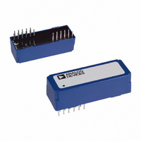
IC LOGIC ISO/3.5KV 0:5IO 22DIP
Manufacturer
Analog Devices Inc
Series
IsoLogic™r
Datasheet
1.AD261AND-0.pdf
(6 pages)
Specifications of AD261BND-0
Rohs Status
RoHS non-compliant
Inputs - Side 1/side 2
2/3
Number Of Channels
5
Isolation Rating
1250Vrms
Voltage - Supply
4 V ~ 5.75 V
Data Rate
40MBd
Propagation Delay
14ns
Output Type
Tri-State
Package / Case
22-DIP Module
Operating Temperature
-25°C ~ 85°C


AD261–SPECIFICATIONS
Parameter
INPUT CHARACTERISTICS
OUTPUT CHARACTERISTICS
DYNAMIC RESPONSE
ISOLATION BARRIER RATING
POWER SUPPLY
TEMPERATURE RANGE
NOTES
1
2
3
4
5
Specifications are subject to change without notice.
For best performance, bypass +5 V dc supplies to com., at or near the device (0.01 F). +5 V dc supplies are also internally bypassed with 0.05 F.
As the supply voltage is applied to either side of the AD261, the internal circuitry will go into a power-up reset mode (all lines disabled) for about 30 s after the point
“Operating” isolation voltage is derived from the Isolation Test Voltage in accordance with such methods as found in VDE-0883 wherein a device will be “hi-pot”
Partial Discharge at 80 pC THLD.
Supply Current will increase slightly, but otherwise the unit will function within specification to –40 C.
where +5 V dc
tested at twice the operating voltage, plus one thousand volts. Partial discharge testing, with an acceptance threshold of 80 pC of discharge may be considered the
same as a hi-pot test (but nondestructive).
Threshold Voltage
Hysteresis Voltage (V
Input Capacitance (C
Input Bias Current (I
Output Voltage
Output Three-State Leakage Current
Max Logic Signal Frequency (f
Waveform Edge Symmetry Error (t
Logic Edge Propagation Delay (t
Minimum Pulsewidth (t
Max Output Update Delay on Fault or After
Operating Isolation Voltage (V
Isolation Rating Test Voltage (V
Transient Immunity (V
Isolation Mode Capacitance (C
Capacitive Leakage Current (I
Supply Voltage (+5 V dc
Power Dissipation Capacitance
Quiescent Supply Current
Supply Current
Rated Performance (T
Storage (T
Positive Transition (V
Negative Transition (V
High Level (V
Low Level (V
Power-Up Reset Interval ( 30 s
STG
SYS & FLD
)
1
OL
OH
)
passes above 3.3 V.
)
IN
H
IN
A
1
TRANSIENT
)
)
)
)
5
(Refer to Figure 2)
SYS
PWMIN
T+
T–
)
and +5 V dc
)
LEAD
)
ISO
CMV
MIN
)
CMV TEST
3
PHL
)
)
)
ERROR
)
, t
PLH
FLD
)
)
4
)
)
Conditions
+5 V dc
+5 V dc
+5 V dc
+5 V dc
+5 V dc
+5 V dc
Per Input
+5 V dc
+5 V dc
+5 V dc
+5 V dc
ENABLE
50% Duty Cycle, +5 V dc
t
AD261A
AD261B
AD261A
AD261B
Total Capacitance, All Lines
240 V rms @ 60 Hz
Rated Performance
Operating
Effective, per Input, Either Side
Effective per Output, Either Side—No Load
Each, +5 V dc
All Lines @ 10 MHz (Sum of +5 V dc
PHL
vs. t
(Typical at T
SYS
SYS
SYS
SYS
SYS
SYS
SYS
SYS
SYS
SYS
PLH
SYS/FLD
= 4.5 V
= 5.5 V
= 4.5 V
= 5.5 V
= 4.5 V
= 5.5 V
= 4.5 V, |I
= 4.5 V, |I
= 4.5 V, |I
= 4.5 V, |I
SYS & FLD
@ Logic Low/High Level Respectively
A
= +25 C, +5 V dc
–2–
O
O
O
O
| = 0.02 mA
| = 4 mA
| = 0.02 mA
| = 4 mA
SYS
= 5 V
SYS & FLD
SYS
, +5 V dc
)
FLD
, t
RR
= 50 ns max unless otherwise noted)
2.0
3.0
0.9
1.2
0.4
0.5
4.4
3.7
20
25
1750
3500
10,000
4.5
4.0
–25
–40
Min
Typ
2.7
3.2
1.8
2.2
0.9
1.0
5
0.5
0.5
14
12
9
8
28
4
18
1
Max
3.15
4.2
2.2
3.0
1.4
1.5
0.1
0.4
25
375
1250
15
2
5.5
5.75
+85
+85
Units
V
V
V
V
V
V
pF
V
V
V
V
MHz
ns
ns
ns
V rms
V rms
V rms
V rms
V/ s
pF
V dc
V dc
pF
mA
mA
REV. 0
pF
C
C
A
A
s
A rms
Related parts for AD261BND-0
Image
Part Number
Description
Manufacturer
Datasheet
Request
R

Part Number:
Description:
±1.7g Dual-Axis IMEMS Accelerometer Evaluation Board
Manufacturer:
Analog Devices Inc
Datasheet:

Part Number:
Description:
Inertial Sensor Evaluation System
Manufacturer:
Analog Devices Inc
Datasheet:
Part Number:
Description:
Manufacturer:
Analog Devices Inc
Datasheet:
Part Number:
Description:
Manufacturer:
Analog Devices Inc
Datasheet:
Part Number:
Description:
Manufacturer:
Analog Devices Inc
Datasheet:
Part Number:
Description:
Manufacturer:
Analog Devices Inc
Datasheet:
Part Number:
Description:
Manufacturer:
Analog Devices Inc
Datasheet:
Part Number:
Description:
Manufacturer:
Analog Devices Inc
Datasheet:
Part Number:
Description:
Manufacturer:
Analog Devices Inc
Datasheet:
Part Number:
Description:
Manufacturer:
Analog Devices Inc
Datasheet:
Part Number:
Description:
Manufacturer:
Analog Devices Inc
Datasheet:
Part Number:
Description:
Manufacturer:
Analog Devices Inc
Datasheet:
Part Number:
Description:
Manufacturer:
Analog Devices Inc
Datasheet: