AD261BND-0 Analog Devices Inc, AD261BND-0 Datasheet - Page 3
AD261BND-0
Manufacturer Part Number
AD261BND-0
Description
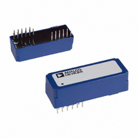
IC LOGIC ISO/3.5KV 0:5IO 22DIP
Manufacturer
Analog Devices Inc
Series
IsoLogic™r
Datasheet
1.AD261AND-0.pdf
(6 pages)
Specifications of AD261BND-0
Rohs Status
RoHS non-compliant
Inputs - Side 1/side 2
2/3
Number Of Channels
5
Isolation Rating
1250Vrms
Voltage - Supply
4 V ~ 5.75 V
Data Rate
40MBd
Propagation Delay
14ns
Output Type
Tri-State
Package / Case
22-DIP Module
Operating Temperature
-25°C ~ 85°C


REV. 0
ABSOLUTE MAXIMUM RATINGS*
Parameter
Supply Voltage (+5 V dc
DC Input Voltage (V
DC Output Voltage (V
Clamp Diode Input Current (I
Clamp Diode Output Current (I
Output DC Current, per Pin (I
DC Current, V
Storage Temperature (T
Lead Temperature (Soldering, 10 sec)
Electrostatic Protection (V
*Stresses above those listed under Absolute Maximum Ratings may cause permanent damage to the device. This is a stress rating only; functional operation of the device
I/O CONFIGURATIONS AVAILABLE
The AD261 is available in several configurations. The choice of
model is determined by the desired number of input vs. output
lines. All models have identical footprints with the power and
enable pins always being in the same locations.
Pin
1–5*
6
7
8
9–14
15
16
17
18–22* F0 Through F4 Digital Xmt or Rcv from S0 Through S4
*Function of pin determined by model. Refer to Table I.
Model
Number
AD261AND-0
AD261AND-1
AD261AND-2
AD261AND-3
AD261AND-4
AD261AND-5
AD261BND-0
AD261BND-1
AD261BND-2
AD261BND-3
AD261BND-4
AD261BND-5
CAUTION
ESD (electrostatic discharge) sensitive device. Electrostatic charges as high as 4000 V readily
accumulate on the human body and test equipment and can discharge without detection.
Although the AD261 features proprietary ESD protection circuitry, permanent damage may
occur on devices subjected to high energy electrostatic discharges. Therefore, proper ESD
precautions are recommended to avoid performance degradation or loss of functionality.
at these or any other conditions above those indicated in the operational sections of this specification is not implied. Exposure to absolute maximum ratings for extended
periods may effect device reliability.
Mnemonic
S0 Through S4 Digital Xmt or Rcv from F0 Through F4
ENABLE
+5 V dc
5 V RTN
5 V RTN
+5 V dc
ENABLE
PIN FUNCTION DESCRIPTIONS
CC
SYS
FLD
or GND (I
SYS
FLD
SYS
FLD
IN MAX
OUT MAX
STG
SYS & FLD
Function
System Output Enable/Three-State
System Power Supply (+5 V dc Input)
System Power Supply Common
Not Present On Unit
Field Power Supply Common
Field Power Supply (+5 V Input)
Field Output Enable/Three-State
ESD
)
CC
)
Description
0 Inputs, 5 Outputs
1 Input, 4 Outputs
2 Inputs, 3 Outputs
3 Inputs, 2 Outputs
4 Inputs, 1 Output
5 Inputs, 0 Outputs
0 Inputs, 5 Outputs
1 Input, 4 Outputs
2 Inputs, 3 Outputs
3 Inputs, 2 Outputs
4 Inputs, 1 Output
5 Inputs, 0 Outputs
)
IK
)
or I
OUT
)
OK
)
GND
)
)
)
Conditions
Referred to +5 V dc
Referred to +5 V RTN
For V
For V
Per MIL-STD-883, Method 3015
I
O
< –0.5 V or V
< –0.5 V or V
ORDERING GUIDE
SYS & FLD
I
O
SYS & FLD
> 5 V RTN
> 5 V RTN
–3–
1.75 kV rms
1.75 kV rms
1.75 kV rms
1.75 kV rms
1.75 kV rms
1.75 kV rms
3.5 kV rms
3.5 kV rms
3.5 kV rms
3.5 kV rms
3.5 kV rms
3.5 kV rms
Isolation
Ratings
and 5 V RTN
and 5 V dc
SYS & FLD
SYS & FLD
ENABLE
5V RTN
SYS & FLD
SYS & FLD
+5V dc
+0.5 V
+0.5 V
FLD
FLD
FLD
F0
F1
F2
F3
F4
PIN CONFIGURATION
Package
Description
Plastic DIP
Plastic DIP
Plastic DIP
Plastic DIP
Plastic DIP
Plastic DIP
Plastic DIP
Plastic DIP
Plastic DIP
Plastic DIP
Plastic DIP
Plastic DIP
Respectively
Respectively
BOTTOM VIEW
15
16
17
18
19
20
21
22
SYSTEM
FIELD
WARNING!
1
2
3
4
5
6
7
8
Min Typ
–0.5
–0.5
–0.5
–25
–25
–25
–50
–40
4.5
S0
S1
S2
S3
S4
ENABLE
+5V dc
5V RTN
5
ESD SENSITIVE DEVICE
SYS
SYS
SYS
AD261
Max
+6.0
+0.5
+0.5
+25
+25
+25
+50
+85
+300
ND-22A
ND-22A
ND-22A
ND-22A
ND-22A
ND-22A
ND-22A
ND-22A
ND-22A
ND-22A
ND-22A
ND-22A
Package
Option
Units
V
V
V
mA
mA
mA
mA
kV
C
C
Related parts for AD261BND-0
Image
Part Number
Description
Manufacturer
Datasheet
Request
R

Part Number:
Description:
±1.7g Dual-Axis IMEMS Accelerometer Evaluation Board
Manufacturer:
Analog Devices Inc
Datasheet:

Part Number:
Description:
Inertial Sensor Evaluation System
Manufacturer:
Analog Devices Inc
Datasheet:
Part Number:
Description:
Manufacturer:
Analog Devices Inc
Datasheet:
Part Number:
Description:
Manufacturer:
Analog Devices Inc
Datasheet:
Part Number:
Description:
Manufacturer:
Analog Devices Inc
Datasheet:
Part Number:
Description:
Manufacturer:
Analog Devices Inc
Datasheet:
Part Number:
Description:
Manufacturer:
Analog Devices Inc
Datasheet:
Part Number:
Description:
Manufacturer:
Analog Devices Inc
Datasheet:
Part Number:
Description:
Manufacturer:
Analog Devices Inc
Datasheet:
Part Number:
Description:
Manufacturer:
Analog Devices Inc
Datasheet:
Part Number:
Description:
Manufacturer:
Analog Devices Inc
Datasheet:
Part Number:
Description:
Manufacturer:
Analog Devices Inc
Datasheet:
Part Number:
Description:
Manufacturer:
Analog Devices Inc
Datasheet: