PC942J00000F Sharp Microelectronics, PC942J00000F Datasheet
PC942J00000F
Specifications of PC942J00000F
Available stocks


Related parts for PC942J00000F


PC942J00000F Summary of contents
Page 1
... PC942J00000F Series ■ Description PC942J00000F Series contains an IRED optically coupled to an OPIC chip packaged pin DIP, available in SMT gullw- ing lead form option. Input-output isolation voltage(rms) is 5.0kV, High speed response ( MAX. 5µs) and CMR is PHL PLH MIN. 10kv/µs. ■ Features 1 ...
Page 2
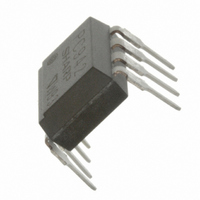
... Internal Connection Diagram Interface ■ Truth table Input O Terminal output Tr High level ON OFF Low level OFF ■ Outline Dimensions 1. Through-Hole [ex. PC942J00000F] ±0.3 1.2 ±0.2 0. ±0.5 9.66 Primary side Date code mark ±0.25 2.54 ±0.1 0.5 Product mass : approx. 0.55g Anode ...
Page 3
... Rank mark There is no rank mark indicator. 2nd digit Month of production Month Mark January 1 February 2 March 3 April 4 May 5 June 6 July 7 August 8 September 9 October O November N December D 3 PC942J00000F Series 3rd digit Week of production Week Mark 1st 1 2nd 2 3rd 3 4th 4 5.6th 5 Sheet No.: D2-A05902EN ...
Page 4
... CM I =5mA, R =470Ω =1kΩ, ∆V =0.5V(MAX) L2 O2H T =25˚C, V =600V(peak =0, R =470Ω =1kΩ, ∆V =0.5V(MAX) L2 O2L 4 PC942J00000F Series (Unless otherwise specified MIN. TYP. MAX. Unit − 1.1 1.4 V 0.6 0.9 − V − − 10 µA − 30 250 pF 5.4 − − ...
Page 5
... Model Line-up Lead Form Through-Hole Sleeve Package 50pcs/sleeve Model No. PC942J00000F Please contact a local SHARP sales representative to inquire about production status. SMT Gullwing Taping 1 000pcs/reel PC942PJ0000F 5 PC942J00000F Series Sheet No.: D2-A05902EN ...
Page 6
... Fig.2 Test Circuit for O Voltage Fig.4 Test Circuit for O 1 O1L Fig.6 Test Circuit for Response Time t =t =0.01µ =50Ω 47Ω V waveform IN V waveform OUT 6 PC942J00000F Series High Level Output O2H 7 Leak Current O2L out PHL PLH 90% ...
Page 7
... Fig.9 Power Dissipation vs. Ambient Temperature 75 80 100 Fig.11 "Low→High" Relative Input Threshold Current vs. Supply Voltage 25 ˚C 0 ˚C −20 ˚C 2.0 2.5 3.0 ( PC942J00000F Series V CM (peak) GND V O2H =5mA F ∆V O2H ∆V O2L V O2L GND =0 F 600 550 500 ...
Page 8
... Ta=25˚C FLH 75 100 Fig. = =10Ω =0.5A O1 0.4A 0.1A 75 100 Fig. =6V CC −0.4A −0.5A 0.001 75 100 8 PC942J00000F Series Low Level Output Voltage vs Output Current =10Ω =5mA F Ta=25˚C 0.1 0.01 0.001 0.01 0.1 O output current I ( High Level Output Voltage vs. 2 ...
Page 9
... Fig.21 Propagation Delay Time vs. Forward Current Ta=−20˚C 25˚C 80˚ (V) CC Fig. = =5Ω =10Ω =5mA F t PLH t PHL 75 100 9 PC942J00000F Series 14 12 Ta=−20˚C 10 25˚C 8 80˚ Supply voltage =5Ω =10Ω Ta=80˚C PHL 3 25˚C −20˚C ...
Page 10
... This application circuit shows the general example of a circuit, and is not a disign guarantee for right opera- tion. Remarks : Please be aware that all data in the graph are just for reference and not for guarantee Power transistor O module GND + 10 PC942J00000F Series Load C E Sheet No.: D2-A05902EN ...
Page 11
... GND level even for instant. Therefore it shall be recommended to design the circuit that electric potential of any pin does not become below GND level. This product is not designed against irradiation and incorporates non-coherent IRED. and GND near the device PC942J00000F Series Sheet No.: D2-A05902EN ...
Page 12
... In the case of long term operation, please take the general IRED degradation (50% degradation over 5 years) into the design consideration. Please decide the input current which become 2 times of MAX. I ● Recommended Foot Print (reference) ✩ For additional design assistance, please review our corresponding Optoelectronic Application Notes. . FLH 8.2 2.2 12 PC942J00000F Series (Unit : mm) Sheet No.: D2-A05902EN ...
Page 13
... Please test the soldering method in actual condition and make sure the soldering works fine, since the impact on the junction between the device and PCB varies depending on the tooling and soldering conditions. Reflow 220˚C or more, 60s or less PC942J00000F Series 4 (min) Sheet No.: D2-A05902EN ...
Page 14
... Specific brominated flame retardants such as the PBBOs and PBBs are not used in this product at all. This product shall not contain the following materials banned in the RoHS Directive (2002/95/EC). •Lead, Mercury, Cadmium, Hexavalent chromium, Polybrominated biphenyls (PBB), Polybrominated diphenyl ethers (PBDE). PC942J00000F Series 14 Sheet No.: D2-A05902EN ...
Page 15
... MAX. 50 pcs. of products shall be packaged in a sleeve. Both ends shall be closed by tabbed and tabless stoppers. The product shall be arranged in the sleeve with its primary side mark on the tabless stopper side. MAX. 20 sleeves in one case. Sleeve outline dimensions 12.0 6.7 PC942J00000F Series 15 (Unit : mm) Sheet No.: D2-A05902EN ...
Page 16
... Direction of product insertion ±0.1 ±0.1 ±0.1 ±0.1 1.75 12.0 2 ±0.05 ±0.1 ±0.1 4.2 10.2 Dimensions List f b Pull-out direction 16 PC942J00000F Series J I (Unit : mm ±0.1 +0.1 4.0 φ1.5 −0 (Unit : mm ±1.5 ±1.0 ±0.5 330 17.5 100 ±1.0 ±0.5 ±0.5 23 2.0 2.0 [Packing : 1 000pcs/reel] Sheet No ...
Page 17
... Measures such as fail-safe function and redundant design should be taken to ensure reliability and safety when SHARP devices are used for or in connection [E224] PC942J00000F Series with equipment that requires higher reliability such as: --- Transportation control and safety equipment (i.e., aircraft, trains, automobiles, etc.) ...