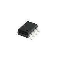
HCPL-2531#520 Avago Technologies US Inc., HCPL-2531#520 Datasheet

HCPL-2531#520
Specifications of HCPL-2531#520
Available stocks
Related parts for HCPL-2531#520
HCPL-2531#520 Summary of contents
Page 1
... Feedback element in switched mode power supplies • High speed logic ground isolation – TTL/TTL, TTL/CMOS, TTL/LSTTL • Replaces pulse transformers • Replaces slow phototransistor isolators • Analog signal ground isolation = 1500 V CM for 1 minute (5000 V rms = 630 V peak for HCPL-4503#060 = 1414 V peak for HCNW devices rms ...
Page 2
... The HCPL-4502, HCPL-0452, and HCNW4502 provide the electrical and switching performance of the 6N136, HCPL- 0501, and HCNW136 with increased ESD protection. The HCPL-4503, HCPL-0453, and HCNW4503 are similar to the HCPL-4502, HCPL-0452, and HCNW4502 optocouplers but have increased common mode transient immunity of 15 kV/µ ...
Page 3
... To order, choose a part number from the part number column and combine with the desired option from the option column to form an order entry. Example 1: HCPL-4502-560E to order product of 300mil DIP Gull Wing Surface Mount package in Tape and Reel packaging with IEC/EN/DIN EN 60747-5-2 Safety Approval in RoHS compliant. Example 2: HCPL-4502 to order product of 300mil DIP package in tube packaging and non RoHS compliant ...
Page 4
... MAX. (0.043 ± 0.013) 2.54 ± 0.25 (0.100 ± 0.010) 8-Pin DIP Package with Gull Wing Surface Mount Option 300 (HCPL-4502/3) 9.65 ± 0.25 (0.380 ± 0.010 (0.250 ± 0.010) ...
Page 5
... Small Outline SO-8 Package (HCPL-0452/ 5.994 ± 0.203 (0.236 ± 0.008) XXX 3.937 ± 0.127 YWW (0.155 ± 0.005) PIN ONE 0.406 ± 0.076 1.270 (0.016 ± 0.003) (0.050) * 5.080 ± 0.127 (0.200 ± 0.005) 3.175 ± 0.127 (0.125 ± 0.005) 1 ...
Page 6
Widebody DIP Package with Gull Wing Surface Mount Option 300 (HCNW4502/3) 11.15 ± 0.15 (0.442 ± 0.006 (0.354 ± 0.006 1.55 (0.061) MAX. 1.78 ± 0.15 (0.070 ± 0.006) 2.54 (0.100) ...
Page 7
Recommended Pb-Free IR Profile * 260 +0/-5°C Tp 217°C TL RAMP-UP 3°C/SEC. MAX. 150 - 200°C T smax T smin ts PREHEAT 60 to 180 SEC 25°C to PEAK TIME Regulatory Information The devices contained in this data ...
Page 8
... IOTM T 175 S I 230 S,INPUT P 600 S,OUTPUT R ≥ Symbol V IORM = 1 sec IOTM S,INPUT P S,OUTPUT R S HCPL-0452/0453 Units I-III 55/100/21 2 560 V peak 1050 V peak 840 V peak 4000 V peak 175 °C 150 mA 600 mW ≥10 Ω 9 Characteristic Units I-IV I-III 55/85/21 2 1414 V peak ...
Page 9
Absolute Maximum Ratings Parameter Storage Temperature Operating Temperature Average Forward Input Current Peak Forward Input Current (50% duty cycle pulse width) (50% duty cycle pulse width) Peak Transient Input Current (≤1 µs pulse width, 300 pps) ...
Page 10
... Electrical Specifications (DC) Over recommended temperature (T A Parameter Symbol Device Current CTR HCPL-4502/3 Transfer Ratio HCPL-0452/3 HCNW4502/3 Logic Low V HCPL-4502/3 OL Output Voltage HCPL-0452/3 HCNW4502/3 Logic High I OH Output Current Logic Low I CCL Supply Current Logic High I CCH Supply Current Input Forward V 8-Pin DIP ...
Page 11
... Logic High at HCNW4502/3 Output Common Mode |CM | HCPL-4502 H Transient Im- HCPL-0452 munity at Logic HCNW4502 High Level HCPL-4503 Output HCPL-0453 HCNW4503 Common Mode |CM | HCPL-4502 L Transient Im- HCPL-0452 munity at Logic HCNW4502 Low Level HCPL-4503 Output HCPL-0453 HCNW4503 *All typicals 25° 0°C to 70°C unless otherwise specified Min ...
Page 12
Package Characteristics Over recommended temperature (T Parameter Sym. Device Input-Output V 8-Pin DIP ISO Momentary SO-8 Withstand Widebody Voltage** 8-Pin DIP (Option 020) I 8-Pin DIP I-O Input-Output R 8-Pin DIP I-O Resistance SO-8 Widebody Input-Output C 8-Pin DIP I-O ...
Page 13
... PIN DIP, SO 25° 5 OUTPUT VOLTAGE - V O Figure 1. DC and pulsed transfer characteristics. 8 PIN DIP, SO-8 1.5 HCPL-4502/3, HCPL-0452/0453 1.0 0.5 0 INPUT CURRENT - mA F Figure 2. Current transfer ratio vs. input current. 8 PIN DIP, SO-8 1000 100 1.0 0.1 0.01 0.001 1 1 FORWARD VOLTAGE - VOLTS F Figure 3 ...
Page 14
... 0 0 25°C A 0.7 HCPL-4502/3, HCPL-0452/0453 0.6 -60 - TEMPERATURE - °C A Figure 4. Current transfer ratio vs. temperature. 8 PIN DIP, SO-8 2000 mA 5 HCPL-4502 1.9kΩ) L 1500 HCPL-0452/3 1000 t PLH 500 - TEMPERATURE - °C A Figure 5. Propagation delay vs. temperature. 8 PIN DIP, SO 1.0 0 25°C A 0.6 ...
Page 15
... I - QUIESCENT INPUT CURRENT - mA F Figure 8. Small-signal current transfer ratio vs. quiescent input current. HCPL-0452/0453/4502/4503 OPTION 060 800 P (mW) S 700 I (mA) For HCPL-4502/4503 S 600 I (mA) For HCPL-0452/0453 S 500 400 300 200 100 100 125 T - CASE TEMPERATURE - °C s Figure 9. Thermal derating curve, dependence of safety limiting value with case temperature per IEC/EN/DIN EN 60747-5-2. ...
Page 16
1 PHL PLH Figure 10. Switching test circuit 10% 90% 90% 10 ...


