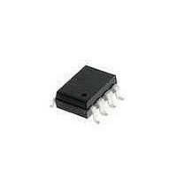
HCPL-2533#300 Avago Technologies US Inc., HCPL-2533#300 Datasheet - Page 8

HCPL-2533#300
Manufacturer Part Number
HCPL-2533#300
Description
OPTOCOUPLER 8-SMD GW
Manufacturer
Avago Technologies US Inc.
Datasheet
1.HCPL-2533500.pdf
(11 pages)
Specifications of HCPL-2533#300
Input Type
DC
Package / Case
8-SMD Gull Wing
Voltage - Isolation
3750Vrms
Number Of Channels
2, Unidirectional
Current - Output / Channel
8mA
Data Rate
250kbps
Propagation Delay High - Low @ If
800ns @ 8mA
Current - Dc Forward (if)
25mA
Output Type
Open Collector
Mounting Type
Surface Mount, Gull Wing
Isolation Voltage
3750 Vrms
Output Device
Phototransistor
Configuration
2 Channel
Current Transfer Ratio
22 %
Maximum Baud Rate
1 MBps
Maximum Forward Diode Voltage
1.7 V
Maximum Reverse Diode Voltage
5 V
Maximum Input Diode Current
25 mA
Maximum Power Dissipation
45 mW
Maximum Operating Temperature
+ 70 C
Minimum Operating Temperature
0 C
Lead Free Status / RoHS Status
Contains lead / RoHS non-compliant
Available stocks
Company
Part Number
Manufacturer
Quantity
Price
Electrical Specifications
Over recommended temperature (T
Parameter
Logic High
Output Current
Logic High
Supply Current
Input Reverse
Breakdown Voltage
Input Capacitance
Input-Output
Insulation Leakage
Current
Resistance
(Input–Output)
Capacitance
(Input–Output)
Input–Input
Insulation Leakage
Current
Resistance
(Input–Input)
Capacitance
(Input–Input)
*All typicals at 25°C.
Notes:
5. Each channel.
6. Current Transfer Ratio is defined as the ratio of output collector current, I
7. Device considered a two-terminal device: Pins 1, 2, 3, and 4 shorted together and Pins 5, 6, 7, and 8 shorted together.
8. Measured between pins 1 and 2 shorted together, and pins 3 and 4 shorted together.
9. Common mode transient immunity in Logic High level is the maximum tolerable (positive) dV
10. The 7.5 k load represents 1 LSTTL unit load of 0.36 mA and a 20 kΩ pull-up resistor.
11. The 4.7 k load represents 1 LSTTL unit load of 0.36 mA and an 8.2 kΩ pull-up resistor.
8
pulse V
the maximum tolerable (negative) dV
in a Logic Low state (i.e., V
CM
, to assure that the output will remain in a Logic High state (i.e., V
O
< 0.8 V).
Symbol
I
I
V
C
I
R
C
I
R
C
OH
CCH
I–O
I–I
R
IN
I–O
I–O
I–I
I–I
CM
A
/dt on the trailing edge of the common mode pulse signal, V
= 0°C to +70°C) unless otherwise specified.
Min.
5
Typ.*
0.5
0.05
60
10
0.6
0.005
10
0.25
12
11
Max.
50
4
1.0
O
, to the forward LED input current, I
O
> 2.0 V). Common mode transient immunity in Logic Low level is
Units
nA
µA
µA
V
pF
µA
Ω
pF
µA
Ω
pF
Test Conditions
T
I
V
I
V
I
V
V
I
f = 1 MHz, V
45% Relative Humidity,
t = 5s
V
T
V
f = 1 MHz
45% Relative Humidity,
t = 5s
V
V
f = 1 MHz
F1
F1
F1
F
A
A
O1
O1
O1
CC
I–O
I–O
I–I
I–I
= 10 µA, T
= 25°C,
= 25°C
CM
= I
= I
= I
= 500 Vdc
= 500 Vdc
= 5.5 V
= V
= V
= V
= 3000 Vdc,
= 500 Vdc
/dt on the leading edge of the common mode
F2
F2
F2
O2
O2
O2
= 0 mA
= mA
= 0 mA
CM
= V
= V
= Open,
, to assure that the output will remain
A
F
= 0 V
= 25°C
CC
CC
F
= 5.5 V
, times 100%.
= 5.5 V
Fig.
5
Note
5
5
5
5
7
7
7
8
8
8


