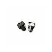
HFBR-1506AM Avago Technologies US Inc., HFBR-1506AM Datasheet - Page 5

HFBR-1506AM
Manufacturer Part Number
HFBR-1506AM
Description
XMITTER FIBER OPTIC SERCOS SMA
Manufacturer
Avago Technologies US Inc.
Datasheet
1.HFBR-2506AM.pdf
(8 pages)
Specifications of HFBR-1506AM
Wavelength
650nm
Spectral Bandwidth
21nm
Voltage - Forward (vf) Typ
2.1V
Current - Dc Forward (if)
60mA
Voltage - Dc Reverse (vr) (max)
3V
Capacitance
60pF
Connector Type
SMA
Function
Fiber Optic Transmitter for SERCOS, SMA Port
Product
Transmitter
Data Rate
16 MBd
Diode Capacitance
60 pF
Maximum Rise Time
15 ns
Maximum Fall Time
15 ns
Operating Supply Voltage
5.5 VDC
Maximum Operating Temperature
+ 85 C
Minimum Operating Temperature
- 40 C
Package / Case
DIP-8
For Use With
Plastic Optical Fiber
Lead Free Status / RoHS Status
Lead free / RoHS Compliant
HFBR-2506AM Receiver
The HFBR-2506AM receiver is housed in a metal-coated,
plastic package, consists of a silicon PIN photodiode
and digitizing IC to produce a logic compatible output.
The IC includes a unique circuit to correct the pulse
width distortion of the first bit after a long idle period.
This enables operation from DC to 16MBd with low
PWD for arbitrary data patterns.
The receiver is a "push-pull" stage compatible with TTL
and CMOS logic. The HFBR-2506AM is compatible with
SMA connectors.
Absolute Maximum Ratings
Notes:
1. 1.6 mm below seating plane.
Electrical Characteristics Table
0 °C to +70 °C, 4.75 V < V
Notes:
1. Typical data are at +25 °C, V
2. BER <= 10E-9, includes a 10.8 dB margin below the receiver switching threshold level (signal to noise ratio =12)
3. Pins 1 and 4 are for mounting and retaining purposes, but are electrically connected, pins 5 and 6 are electrically isolated. It is recommended
5
Parameter
Storage and Operating Temperature
Supply Voltage
Average Output Current
Output Power Dissipation
Lead Soldering Cycle
Temp
Time
Parameter
Peak Input Power Level Logic HIGH
Peak Input Power Level Logic LOW
Supply Current
High Level Output Voltage
Low Level Output Voltage
Pulse Width Distortion
Propagation Delay Time
that pins 1, 4, 5 and 6 all be connected to ground to reduce coupling of elecrical noise
CC
CC
= 5.0 V
< 5.25 V, V
Symbol
I
P
T
V
T
T
O
OD
S
SOL
SOL
CC
,
,
AVG
O
Symbol
P
P
I
V
V
PWD
T
_LH
CC
RH
RL
P_HL
OH
OH
P-P
or
Noise < = 100 mV unless otherwise noted.
Min
-20
-22
4.2
-19
Min
-40
-0.5
27
4.7
0.22
Typ
1
Figure 6.
BOTTOM VIEW,
SEE NOTE 4
HFBR-2506AM
4
1
Max
16
10
+85
5.5
80
260
Max
19
150
-42
-44
-2
-10
45
0.4
5
6
7
8
Unit
mA
ns
ns
dBm
dBm
V
V
Unit
°C
V
mA
mW
°C
s
PIN
1
4
5
6
7
8
|PWD| < 19 ns
Condition
1 mm POF
1 mm POF
I
I
200 µm HCS
200 µm HCS
V
O
O
O
= 40 µA
= 1.6 mA
= Open
CONNECTED TO PIN 4
CONNECTED TO PIN 1
NO CONNECT
VCC
GND
VO
FUNCTION
Notes
1
Notes
2


