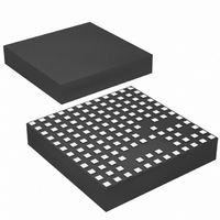
LTM4606IV#PBF Linear Technology, LTM4606IV#PBF Datasheet - Page 14

LTM4606IV#PBF
Manufacturer Part Number
LTM4606IV#PBF
Description
IC DC/DC UMODULE 6A 133-LGA
Manufacturer
Linear Technology
Series
µModuler
Type
Point of Load (POL) Non-Isolatedr
Specifications of LTM4606IV#PBF
Design Resources
LTM4606 Spice Model
Output
0.6 ~ 5 V
Number Of Outputs
1
Power (watts)
30W
Mounting Type
Surface Mount
Voltage - Input
4.5 ~ 28 V
Package / Case
133-LGA
1st Output
0.6 ~ 5 VDC @ 6A
Size / Dimension
0.59" L x 0.59" W x 0.11" H (15mm x 15mm x 2.8mm)
Power (watts) - Rated
30W
Operating Temperature
-40°C ~ 125°C
Efficiency
93%
Dc To Dc Converter Type
Non-Inverting/Inverting/Step Up/Step Down
Pin Count
133
Input Voltage
28V
Output Voltage
0.6 to 5V
Switching Freq
900KHz
Output Current
6A
Package Type
LGA
Isolation Voltage
Not RequiredV
Output Type
Adjustable
Switching Regulator
Yes
Load Regulation
0.3%
Line Regulation
0.3%
Mounting
Surface Mount
Input Voltage (min)
4.5V
Operating Temperature Classification
Automotive
Lead Free Status / RoHS Status
Lead free / RoHS Compliant
3rd Output
-
2nd Output
-
Lead Free Status / Rohs Status
Compliant
Available stocks
Company
Part Number
Manufacturer
Quantity
Price
applicaTions inForMaTion
LTM4606
Output Voltage Tracking
Output voltage tracking can be programmed externally
using the TRACK/SS pin. The output can be tracked up and
down with another regulator. Figure 4 shows an example
of coincident tracking where the master regulator’s output
is divided down with an external resistor divider that is the
same as the slave regulator’s feedback divider. Ratiometric
modes of tracking can be achieved by selecting different
resistor values to change the output tracking ratio. The
master output must be greater than the slave output for
the tracking to work. Figure 5 shows the coincident output
tracking characteristics.
14
CONTROL
MASTER
OUTPUT
TRACK
VOLTAGE
OUTPUT
Figure 5. Coincident Tracking Characteristics
Figure 4. Output Voltage Coincident Tracking
V
C
IN
R2
60.4k
R1
19.1k
IN
100k
V
PGOOD
RUN
COMP
INTV
DRV
f
TRACK/SS
SET
D
CC
CC
SGND
LTM4606
V
IN
TIME
PLLIN
PGND
MASTER OUTPUT
MARG0
MARG1
SLAVE OUTPUT
MPGM
V
FCB
OUT
V
FB
4606 F05
4606 F04
19.1k
C
OUT
SLAVE
OUTPUT
2.5V
Run Enable
The RUN pin is used to enable the power module. The
pin has an internal 5.1V zener to ground. The pin can be
driven with a logic input not to exceed 5V.
The RUN pin can also be used as an undervoltage lock out
(UVLO) function by connecting a resistor divider from the
input supply to the RUN pin:
where R2 is the bottom resistor of the divider, R1 is the
top resistor of the divider.
Power Good
The PGOOD pin is an open-drain pin that can be used to
monitor valid output voltage regulation. This pin monitors
a ±10% window around the regulation point and tracks
with margining.
COMP Pin
This pin is the external compensation pin. The module
has already been internally compensated for most output
voltages. Table 2 is provided for most application require-
ments. LTpowerCAD™ is available for other control loop
optimization.
FCB Pin
The FCB pin determines whether the bottom MOSFET
remains on when current reverses in the inductor. Tying
this pin above its 0.6V threshold enables discontinuous
operation where the bottom MOSFET turns off when in-
ductor current reverses. FCB pin below the 0.6V threshold
forces continuous synchronous operation, allowing current
to reverse at light loads and maintain low output ripple.
V
UVLO
=
R1+ R2
R2
• 1.5V
4606fb


