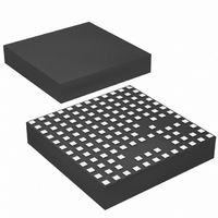
LTM4606IV#PBF Linear Technology, LTM4606IV#PBF Datasheet - Page 19

LTM4606IV#PBF
Manufacturer Part Number
LTM4606IV#PBF
Description
IC DC/DC UMODULE 6A 133-LGA
Manufacturer
Linear Technology
Series
µModuler
Type
Point of Load (POL) Non-Isolatedr
Specifications of LTM4606IV#PBF
Design Resources
LTM4606 Spice Model
Output
0.6 ~ 5 V
Number Of Outputs
1
Power (watts)
30W
Mounting Type
Surface Mount
Voltage - Input
4.5 ~ 28 V
Package / Case
133-LGA
1st Output
0.6 ~ 5 VDC @ 6A
Size / Dimension
0.59" L x 0.59" W x 0.11" H (15mm x 15mm x 2.8mm)
Power (watts) - Rated
30W
Operating Temperature
-40°C ~ 125°C
Efficiency
93%
Dc To Dc Converter Type
Non-Inverting/Inverting/Step Up/Step Down
Pin Count
133
Input Voltage
28V
Output Voltage
0.6 to 5V
Switching Freq
900KHz
Output Current
6A
Package Type
LGA
Isolation Voltage
Not RequiredV
Output Type
Adjustable
Switching Regulator
Yes
Load Regulation
0.3%
Line Regulation
0.3%
Mounting
Surface Mount
Input Voltage (min)
4.5V
Operating Temperature Classification
Automotive
Lead Free Status / RoHS Status
Lead free / RoHS Compliant
3rd Output
-
2nd Output
-
Lead Free Status / Rohs Status
Compliant
Available stocks
Company
Part Number
Manufacturer
Quantity
Price
applicaTions inForMaTion
Table 3. 1.5V Output
DERATING CURVE
Figures 8, 10
Figures 8, 10
Figures 8, 10
Figures 9, 11
Figures 9, 11
Figures 9, 11
Table 4. 3.3V Output
DERATING CURVE
Figures 12, 14
Figures 12, 14
Figures 12, 14
Figures 13, 15
Figures 13, 15
Figures 13, 15
Heat Sink Manufacturer
Wakefield Engineering
Layout Checklist/Example
The high integration of LTM4606 makes the PCB board
layout very simple and easy. However, to optimize its
electrical and thermal performance, some layout con-
siderations are still necessary.
• Use large PCB copper areas for high current path, in-
• Place high frequency ceramic input and output capaci-
• Place a dedicated power ground layer underneath the
• Use round corners for the PCB copper layer to minimize
• To minimize the EMI noise and reduce module thermal
• Do not put vias directly on pads, unless they are capped.
cluding V
PCB conduction loss and thermal stress.
tors next to the V
high frequency noise.
unit.
the radiated noise.
stress, use multiple vias for interconnection between
top layer and other power layers on different locations.
IN
, PGND and V
D
, PGND and V
V
V
12, 24
12, 24
12, 24
12, 24
12, 24
12, 24
5, 12
5, 12
5, 12
5, 12
5, 12
5, 12
IN
IN
OUT
(V)
(V)
. It helps to minimize the
OUT
pins to minimize
Part No: LTN20069
POWER LOSS CURVE
POWER LOSS CURVE
Figure 6
Figure 6
Figure 6
Figure 6
Figure 6
Figure 6
Figure 7
Figure 7
Figure 7
Figure 7
Figure 7
Figure 7
• Use a separated SGND ground copper area for com-
• Place one or more high frequency ceramic capacitors
Figure 17 gives a good example of the recommended
layout. For load current below 3A, decouple the input and
output grounds. Use vias to connect GND pads to the
bottom layer, then connect to the right side of the module
as the output GND.
AIR FLOW (LFM)
AIR FLOW (LFM)
ponents connected to signal pins. Connect the SGND
to PGND underneath the unit.
close to the connection into the system board.
V
GND
V
OUT
IN
200
400
200
400
200
400
200
400
0
0
0
0
C
OUT
C
IN
Figure 17. Recommended PCB Layout
C
OUT
C
IN
Phone: 603-635-2800
BGA Heat Sink
BGA Heat Sink
BGA Heat Sink
BGA Heat Sink
BGA Heat Sink
BGA Heat Sink
HEAT SINK
HEAT SINK
None
None
None
None
None
None
LTM4606
θ
θ
JA
JA
13.5
13.5
9.5
(°C/W)
10
(°C/W)
11
10
10
4606 F17
9
7
5
7
5
19
SIGNAL
GND
4606fb


