MA330013 Microchip Technology, MA330013 Datasheet - Page 146
MA330013
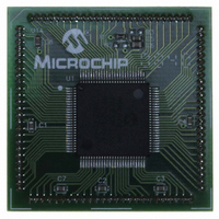
Manufacturer Part Number
MA330013
Description
MODULE PLUG-IN DSPIC33 100TQFP
Manufacturer
Microchip Technology
Specifications of MA330013
Accessory Type
Plug-In Module (PIM) - dsPIC33FJ256MC710
Tool / Board Applications
General Purpose MCU, MPU, DSP, DSC
Mcu Supported Families
DsPIC33
Silicon Manufacturer
Microchip
Core Architecture
DsPIC
Core Sub-architecture
DsPIC33
Silicon Core Number
DsPIC33F
Silicon Family Name
DsPIC33FJxxMCxxx
Rohs Compliant
Yes
For Use With
DM330023 - BOARD DEV DSPICDEM MCHV
Lead Free Status / RoHS Status
Not applicable / Not applicable
For Use With/related Products
Explorer 16 (DM240001 or DM240002)
Lead Free Status / RoHS Status
Lead free / RoHS Compliant, Not applicable / Not applicable


dsPIC33F
REGISTER 7-7:
DS70165E-page 144
bit 15
bit 7
Legend:
R = Readable bit
-n = Value at POR
bit 15
bit 14
bit 13
bit 12
bit 11
bit 10
bit 9
bit 8
bit 7
bit 6
bit 5
bit 4
PWCOL7
XWCOL7
R/C-0
R/C-0
PWCOL7: Channel 7 Peripheral Write Collision Flag bit
1 = Write collision detected
0 = No write collision detected
PWCOL6: Channel 6 Peripheral Write Collision Flag bit
1 = Write collision detected
0 = No write collision detected
PWCOL5: Channel 5 Peripheral Write Collision Flag bit
1 = Write collision detected
0 = No write collision detected
PWCOL4: Channel 4 Peripheral Write Collision Flag bit
1 = Write collision detected
0 = No write collision detected
PWCOL3: Channel 3 Peripheral Write Collision Flag bit
1 = Write collision detected
0 = No write collision detected
PWCOL2: Channel 2 Peripheral Write Collision Flag bit
1 = Write collision detected
0 = No write collision detected
PWCOL1: Channel 1 Peripheral Write Collision Flag bit
1 = Write collision detected
0 = No write collision detected
PWCOL0: Channel 0 Peripheral Write Collision Flag bit
1 = Write collision detected
0 = No write collision detected
XWCOL7: Channel 7 DMA RAM Write Collision Flag bit
1 = Write collision detected
0 = No write collision detected
XWCOL6: Channel 6 DMA RAM Write Collision Flag bit
1 = Write collision detected
0 = No write collision detected
XWCOL5: Channel 5 DMA RAM Write Collision Flag bit
1 = Write collision detected
0 = No write collision detected
XWCOL4: Channel 4 DMA RAM Write Collision Flag bit
1 = Write collision detected
0 = No write collision detected
PWCOL6
XWCOL6
R/C-0
R/C-0
DMACS0: DMA CONTROLLER STATUS REGISTER 0
W = Writable bit
‘1’ = Bit is set
PWCOL5
XWCOL5
R/C-0
R/C-0
PWCOL4
XWCOL4
R/C-0
R/C-0
Preliminary
U = Unimplemented bit, read as ‘0’
‘0’ = Bit is cleared
PWCOL3
XWCOL3
R/C-0
R/C-0
PWCOL2
XWCOL2
R/C-0
R/C-0
© 2007 Microchip Technology Inc.
x = Bit is unknown
PWCOL1
XWCOL1
R/C-0
R/C-0
PWCOL0
XWCOL0
R/C-0
R/C-0
bit 8
bit 0
Related parts for MA330013
Image
Part Number
Description
Manufacturer
Datasheet
Request
R

Part Number:
Description:
Manufacturer:
Microchip Technology Inc.
Datasheet:
Part Number:
Description:
Manufacturer:
Microchip Technology Inc.
Datasheet:
Part Number:
Description:
Manufacturer:
Microchip Technology Inc.
Datasheet:
Part Number:
Description:
Manufacturer:
Microchip Technology Inc.
Datasheet:
Part Number:
Description:
Manufacturer:
Microchip Technology Inc.
Datasheet:
Part Number:
Description:
Manufacturer:
Microchip Technology Inc.
Datasheet:
Part Number:
Description:
Manufacturer:
Microchip Technology Inc.
Datasheet:
Part Number:
Description:
Manufacturer:
Microchip Technology Inc.
Datasheet: