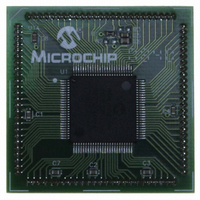
MA330013 Microchip Technology, MA330013 Datasheet - Page 269

MA330013
Manufacturer Part Number
MA330013
Description
MODULE PLUG-IN DSPIC33 100TQFP
Manufacturer
Microchip Technology
Specifications of MA330013
Accessory Type
Plug-In Module (PIM) - dsPIC33FJ256MC710
Tool / Board Applications
General Purpose MCU, MPU, DSP, DSC
Mcu Supported Families
DsPIC33
Silicon Manufacturer
Microchip
Core Architecture
DsPIC
Core Sub-architecture
DsPIC33
Silicon Core Number
DsPIC33F
Silicon Family Name
DsPIC33FJxxMCxxx
Rohs Compliant
Yes
For Use With
DM330023 - BOARD DEV DSPICDEM MCHV
Lead Free Status / RoHS Status
Not applicable / Not applicable
For Use With/related Products
Explorer 16 (DM240001 or DM240002)
Lead Free Status / RoHS Status
Lead free / RoHS Compliant, Not applicable / Not applicable
- Current page: 269 of 370
- Download datasheet (6Mb)
21.3.14
The amount of data that is buffered between interrupts
is determined by the Buffer Length (BLEN<1:0>) con-
trol bits in the DCICON2 SFR. The size of the transmit
and receive buffers can vary from 1 to 4 data words
using the BLEN control bits. The BLEN control bits are
compared to the current value of the DCI buffer control
unit address counter. When the 2 LSbs of the DCI
address counter match the BLEN<1:0> value, the
buffer control unit will be reset to ‘0’. In addition, the
contents of the Receive Shadow registers are trans-
ferred to the Receive Buffer registers and the contents
of the Transmit Buffer registers are transferred to the
Transmit Shadow registers.
21.3.15
There is no direct coupling between the position of the
AGU Address Pointer and the data frame boundaries.
This means that there will be an implied assignment of
each transmit and receive buffer that is a function of the
BLEN control bits and the number of enabled data slots
via the TSE and RSE control bits.
As an example, assume that a 4-word data frame is
chosen and that we want to transmit on all four time
slots in the frame. This configuration would be estab-
lished by setting the TSE0, TSE1, TSE2 and TSE3
control bits in the TSCON SFR. With this module setup,
the TXBUF0 register would naturally be assigned to
slot #0, the TXBUF1 register would naturally be
assigned to slot #1, and so on.
© 2007 Microchip Technology Inc.
Note:
Note 1: DCI can trigger a DMA data transfer. If
2: If DMA transfers are required, the DCI
BUFFER ALIGNMENT WITH DATA
FRAMES
When more than four time slots are active
within a data frame, the user code must
keep track of which time slots are to be
read/written at each interrupt. In some
cases, the alignment between transmit/
receive buffers and their respective slot
assignments could be lost. Examples of
such cases include an emulation break-
point or a hardware trap. In these
situations, the user should poll the SLOT
status bits to determine what data should
be loaded into the buffer registers to
resynchronize the software with the DCI
module.
BUFFER LENGTH CONTROL
DCI is selected as a DMA IRQ source, a
DMA transfer occurs when the DCIIF bit
gets set as a result of a DCI transmission
or reception.
TX/RX buffer must be set to a size of
1 word (i.e., BLEN<1:0> = 00).
Preliminary
21.3.16
There are two transmit status bits in the DCISTAT SFR.
The TMPTY bit is set when the contents of the transmit
buffer registers are transferred to the transmit shadow
registers. The TMPTY bit may be polled in software to
determine when the transmit buffer registers may be
written. The TMPTY bit is cleared automatically by the
hardware when a write to one of the four transmit
buffers occurs.
The TUNF bit is read-only and indicates that a transmit
underflow has occurred for at least one of the transmit
buffer registers that is in use. The TUNF bit is set at the
time the transmit buffer registers are transferred to the
transmit shadow registers. The TUNF status bit is
cleared automatically when the buffer register that
underflowed is written by the CPU.
21.3.17
There are two receive status bits in the DCISTAT SFR.
The RFUL status bit is read-only and indicates that new
data is available in the receive buffers. The RFUL bit is
cleared automatically when all receive buffers in use
have been read by the CPU.
The ROV status bit is read-only and indicates that a
receive overflow has occurred for at least one of the
receive buffer locations. A receive overflow occurs
when the buffer location is not read by the CPU before
new data is transferred from the shadow registers. The
ROV status bit is cleared automatically when the buffer
register that caused the overflow is read by the CPU.
When a receive overflow occurs for a specific buffer
location, the old contents of the buffer are overwritten.
Note:
Note:
TRANSMIT STATUS BITS
The transmit status bits only indicate
status for buffer locations that are used by
the module. If the buffer length is set to
less than four words, for example, the
unused buffer locations will not affect the
transmit status bits.
RECEIVE STATUS BITS
The receive status bits only indicate status
for buffer locations that are used by the
module. If the buffer length is set to less
than four words, for example, the unused
buffer locations will not affect the transmit
status bits.
dsPIC33F
DS70165E-page 267
Related parts for MA330013
Image
Part Number
Description
Manufacturer
Datasheet
Request
R

Part Number:
Description:
Manufacturer:
Microchip Technology Inc.
Datasheet:

Part Number:
Description:
Manufacturer:
Microchip Technology Inc.
Datasheet:

Part Number:
Description:
Manufacturer:
Microchip Technology Inc.
Datasheet:

Part Number:
Description:
Manufacturer:
Microchip Technology Inc.
Datasheet:

Part Number:
Description:
Manufacturer:
Microchip Technology Inc.
Datasheet:

Part Number:
Description:
Manufacturer:
Microchip Technology Inc.
Datasheet:

Part Number:
Description:
Manufacturer:
Microchip Technology Inc.
Datasheet:

Part Number:
Description:
Manufacturer:
Microchip Technology Inc.
Datasheet:


