HSC-ADC-EVALCZ Analog Devices Inc, HSC-ADC-EVALCZ Datasheet - Page 9
HSC-ADC-EVALCZ
Manufacturer Part Number
HSC-ADC-EVALCZ
Description
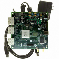
KIT EVAL ADC FIFO HI SPEED
Manufacturer
Analog Devices Inc
Datasheets
1.HSC-ADC-EVALB-DCZ.pdf
(28 pages)
2.HSC-ADC-EVALCZ.pdf
(32 pages)
3.HSC-ADC-EVALCZ.pdf
(40 pages)
Specifications of HSC-ADC-EVALCZ
Design Resources
EVALC PC Board Gerber File
Accessory Type
ADC Interface Board
Silicon Manufacturer
Analog Devices
Application Sub Type
ADC
Kit Application Type
Data Converter
Features
Buffer Memory Board For Capturing Digital Data, USB Port Interface, Windows 98, Windows 2000
Kit Contents
ADC Analyzer, Buffer Memory Board
Rohs Compliant
Yes
Lead Free Status / RoHS Status
Lead free / RoHS Compliant
For Use With/related Products
Single ADC Version
Lead Free Status / Rohs Status
Supplier Unconfirmed
Available stocks
Company
Part Number
Manufacturer
Quantity
Price
Company:

Part Number:
HSC-ADC-EVALCZ
Manufacturer:
Analog Devices Inc
Quantity:
135


THEORY OF OPERATION
The FIFO evaluation board can be divided into several circuits,
each of which plays an important part in acquiring digital data
from the ADC and allows the PC to upload and process that
data. The evaluation kit is based around the IDT72V283 FIFO
chip from Integrated Device Technology, Inc (IDT). The system
can acquire digital data at speeds up to 133 MSPS and data
record lengths up to 32 kB using the HSC-ADC-EVALB-SC
FIFO evaluation kit. The HSC-ADC-EVALB-DC, which has
two FIFO chips, is available to evaluate multichannel ADCs or
demultiplexed data from ADCs sampling faster than 133 MSPS.
A USB 2.0 microcontroller communicating with ADC Analyzer
allows for easy interfacing to newer computers using the USB 2.0
(USB 1.1-compatible) interface.
The process of filling the FIFO chip or chips and reading the
data back requires several steps. First, ADC Analyzer initiates
the FIFO chip fill process. The FIFO chips are reset, using a
master reset signal (MRS). The USB microcontroller is then
suspended, which turns off the USB oscillator and ensures that
it does not add noise to the ADC input. After the FIFO chips
completely fill, the full flags from the FIFO chips send a signal
to the USB microcontroller to wake up the microcontroller
from suspend. ADC Analyzer waits for approximately 30 ms
and then begins the readback process.
During the readback process, the acquisition of data from
FIFO 1 (U201) or FIFO 2 (U101) is controlled via Signal OEA
and Signal OEB. Because the data outputs of both FIFO chips
drive the same 16-bit data bus, the USB microcontroller
controls the OEA and OEB signals to read data from the correct
FIFO chip. From an application standpoint, ADC Analyzer
sends commands to the USB microcontroller to initiate a read
from the correct FIFO chip, or from both FIFO chips in dual or
demultiplexed mode.
CLOCKING DESCRIPTION
Each channel of the buffer memory requires a clock signal to
capture data. These clock signals are normally provided by the
ADC evaluation board and are passed along with the data
through Connector J104 (Pin 37 for both Channel A and
Channel B). If only a single clock is passed for both channels,
they can be connected together by Jumper J303.
Jumpers J304 and J305 at the output of the LVDS receiver allow
the output clock to be inverted by the LVDS receiver. By default,
the clock outputs are inverted by the LVDS receiver.
The single-ended clock signal from each data channel is
buffered and converted to a differential CMOS signal by two
gates of a low voltage differential signal (LVDS) receiver, U301.
This allows the clock source for each channel to be CMOS,
TTL, or ECL.
Rev. 0 | Page 9 of 28
HSC-ADC-EVALB-SC/HSC-ADC-EVALB-DC
The clock signals are ac-coupled by 0.1 μF capacitors.
Potentiometer R312 and Potentiometer R315 allow for fine
tuning the threshold of the LVDS gates. In applications where
fine-tuning the threshold is critical, these potentiometers can be
replaced with a higher resistance value to increase the
adjustment range. Resistors R301, R302, R303, R304, R311,
R313, R314, and R316 set the static input to each of the
differential gates to a dc voltage of approximately 1.5 V.
At assembly, Solder Jumper J310 to Solder Jumper J313 are set
to bypass the potentiometer. For fine adjustment using the pot,
the solder jumpers must be removed, and R312 and R315 must
be populated.
U302, an XOR gate array, is included in the design to let users
add gate delays to the FIFO memory chip clock paths. They are
not required under normal conditions and are bypassed at
assembly by Jumper J314 and Jumper J315. Jumper J306 and
Jumper J307 allow the clock signals to be inverted through an
XOR gate. In the default setting, the clocks are not inverted by
the XOR gate.
The clock paths described above determine the WRT_CLK1 and
WRT_CLK2 signals at each FIFO memory chip (U101 and
U201). The timing options above should let you choose a clock
signal that meets the setup and hold time requirements to
capture valid data.
A clock generator can be applied directly to S1 and/or S3. This
clock generator should be the same unit that provides the clock
for the ADC. These clock paths are ac-coupled, so that a sine
wave generator can be used. DC bias can be adjusted by
R301/R302 and R303/R304.
The DS90LV048A differential line receiver is used to square the
clock signal levels applied externally to the FIFO evaluation
board. The output of this clock receiver can either directly drive
the write clock of the IDT72V283 FIFO(s), or first pass through
the XOR gate timing circuitry described above.
SPI DESCRIPTION
The Cypress IC (U502) supports the HSC SPI standard to allow
programming of ADCs that have SPI-accessible register maps.
U102 is a buffer that drives the 4-wire SPI (SCLK, SDI, SDO,
CSB
row. J502 is an auxiliary SPI connector to monitor the SPI
signals connected directly to the Cypress IC. For more
information on this and other functions, consult the user
manual titled Interfacing to High Speed ADCs via SPI at
www.analog.com/hsc-FIFO.
1
Note that CSB1 is the default CSB line used.
1
) through the 120-pin connector (J104) on the third or top
Related parts for HSC-ADC-EVALCZ
Image
Part Number
Description
Manufacturer
Datasheet
Request
R

Part Number:
Description:
KIT EVAL ADC FIFO DUAL-CH USB HS
Manufacturer:
Analog Devices Inc
Datasheet:

Part Number:
Description:
KIT EVAL ADC USB FIFO HI-SPEED
Manufacturer:
Analog Devices Inc
Datasheet:

Part Number:
Description:
BOARD FPGA OCTAL LVDS FOR ADC
Manufacturer:
Analog Devices Inc
Datasheet:
Part Number:
Description:
KIT EVAL FOR SINGLE CHAN HSC ADC
Manufacturer:
Analog Devices Inc

Part Number:
Description:
KIT EVAL FOR DUAL ADC/CONV
Manufacturer:
Analog Devices Inc
Datasheet:
Part Number:
Description:
KIT EVAL ADC USB FIFO HI-SPEED
Manufacturer:
Analog Devices Inc
Datasheet:

Part Number:
Description:
KIT EVAL ADC USB FIFO HI-SPEED
Manufacturer:
Analog Devices Inc
Datasheet:
Part Number:
Description:
KIT EVAL ADC FIFO DUAL-CH USB HS
Manufacturer:
Analog Devices Inc
Datasheet:
Part Number:
Description:
BOARD FPGA QUAD LVDS FOR ADC
Manufacturer:
Analog Devices Inc
Datasheet:
Part Number:
Description:
Adapter For AD922x Family
Manufacturer:
Analog Devices Inc
Datasheet:
Part Number:
Description:
Interposer Quad/octal ADCs
Manufacturer:
Analog Devices Inc
Datasheet:

Part Number:
Description:
±1.7g Dual-Axis IMEMS Accelerometer Evaluation Board
Manufacturer:
Analog Devices Inc
Datasheet:

Part Number:
Description:
IC MULTIPLIER ANALOG 8-SOIC T/R
Manufacturer:
Analog Devices Inc
Datasheet:
Part Number:
Description:
IC ANALOG MULTIPLIER 8-DIP
Manufacturer:
Analog Devices Inc
Datasheet: