AC164337 Microchip Technology, AC164337 Datasheet - Page 187
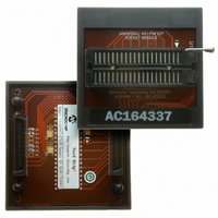
AC164337
Manufacturer Part Number
AC164337
Description
MODULE SOCKET FOR PM3 40DIP
Manufacturer
Microchip Technology
Datasheet
1.AC164335.pdf
(286 pages)
Specifications of AC164337
Module/board Type
Socket Module - DIP
Product
Microcontroller Accessories
Lead Free Status / RoHS Status
Not applicable / Not applicable
For Use With/related Products
MPLAB® PM3
Lead Free Status / RoHS Status
Lead free / RoHS Compliant, Not applicable / Not applicable


EXAMPLE 16-1:
16.15 Changing A/D Clock
In general, the ADC cannot accept changes to the ADC
clock divisor while ADON = 1. If the user makes A/D
clock changes while ADON = 1, the results will be
indeterminate.
16.16 Sample and Conversion
The ADC module always assigns two ADC clock peri-
ods for the sampling process. When operating at the
maximum conversion rate of 2 Msps per channel, the
sampling period is:
© 2006 Microchip Technology Inc.
; The actual pair conversion interrupt handler
; Don't forget to pop the stack when done and return from interrupt
ADC_PAIR0_PROC:
ADC_PAIR1_PROC:
ADC_PAIR2_PROC:
ADC_PAIR3_PROC:
ADC_PAIR4_PROC:
ADC_PAIR5_PROC:
2 x 41.6 nsec = 83.3 nsec.
...
POP.S
RETFIE
...
POP.S
RETFIE
...
POP.S
RETFIE
...
POP.S
RETFIE
...
POP.S
RETFIE
...
POP.S
RETFIE
ADC BASE REGISTER CODE (CONTINUED)
; The ADC pair 0 conversion complete handler
; Restore W0-W3 and SR registers
; Return from Interrupt
; The ADC pair 1 conversion complete handler
; Restore W0-W3 and SR registers
; Return from Interrupt
; The ADC pair 2 conversion complete handler
; Restore W0-W3 and SR registers
; Return from Interrupt
; The ADC pair 3 conversion complete handler
; Restore W0-W3 and SR registers
; Return from Interrupt
; The ADC pair 4 conversion complete handler
; Restore W0-W3 and SR registers
; Return from Interrupt
; The ADC pair 5 conversion complete handler
; Restore W0-W3 and SR registers
; Return from Interrupt
Preliminary
Each ADC pair specified in the ADCPCx registers ini-
tiates a sample operation when the selected trigger
event occurs. The conversion of the sampled analog
data occurs as resources become available.
If a new trigger event occurs for a specific channel
before a previous sample and convert request for that
channel has been processed, the newer request is
ignored. It is the user’s responsibility not to exceed the
conversion rate capability for the module.
The actual conversion process requires 10 additional
ADC clocks. The conversion is processed serially, bit 9
first, then bit 8, down to bit 0. The result is stored when
the conversion is completed.
dsPIC30F1010/202X
DS70178C-page 185
Related parts for AC164337
Image
Part Number
Description
Manufacturer
Datasheet
Request
R

Part Number:
Description:
Manufacturer:
Microchip Technology Inc.
Datasheet:
Part Number:
Description:
Manufacturer:
Microchip Technology Inc.
Datasheet:
Part Number:
Description:
Manufacturer:
Microchip Technology Inc.
Datasheet:
Part Number:
Description:
Manufacturer:
Microchip Technology Inc.
Datasheet:
Part Number:
Description:
Manufacturer:
Microchip Technology Inc.
Datasheet:
Part Number:
Description:
Manufacturer:
Microchip Technology Inc.
Datasheet:
Part Number:
Description:
Manufacturer:
Microchip Technology Inc.
Datasheet:
Part Number:
Description:
Manufacturer:
Microchip Technology Inc.
Datasheet: