VDIP1 FTDI, Future Technology Devices International Ltd, VDIP1 Datasheet - Page 10
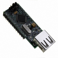
VDIP1
Manufacturer Part Number
VDIP1
Description
MOD MCU-USB HOST CTLR 24-DIP
Manufacturer
FTDI, Future Technology Devices International Ltd
Series
Vinculumr
Datasheet
1.VDIP1.pdf
(23 pages)
Specifications of VDIP1
Main Purpose
Interface, USB 2.0 Host/Controller
Embedded
Yes, ASIC
Utilized Ic / Part
VNC1L-1A
Primary Attributes
Single A-Type Connector, UART / Parallel FIFO / SPI Interfaces
Secondary Attributes
Second USB Port is Available via Pins, Traffic LEDs
Lead Free Status / RoHS Status
Lead free / RoHS Compliant
Other names
768-1001


3.6 Signal Descriptions – Serial Peripheral Interface (SPI)
The SPI I/O pin description of the VNC1L device are shown in
Pins No
Table 3.5 - Data and Control Bus Signal Mode Options – SPI Slave Interface
When in SPI mode, the timing of a read operation is shown in Figure 3.3
From Start - SPI CS must be held high for the entire read cycle, and must be taken low for at least one
clock period after t he read is co mpleted. The first bit on SPI Data In is the R/W bit - inputting a ‘1’ here
a llows data to be read fro m the chip. The next bit is the address bit, ADD, which is used to indicate
whether the data register (‘0’) or the status register (‘1’) is read from. During the SPI read cycle a byte of
data will start being output on SPI Data Out on the next clock cycle after t he address bit, MSBAfterfirst.t
he data has been clocked out of the chip, t he status of SPI Data. Out should be checked to see if the
data read is new data. A ‘0’ level here on SPI Data Out means that the data read is new data. A ‘1’
indicates that the data read is old data, and the read cycle should be repeated to get new data.
Remember that CS must be held low for at least one clock period before being taken high again to
continue with the next read or write cycle.
6
8
9
10
Figure 3.3 – SPI Slave Data Read Cycle.
3.6.1 SPI Slave Data Read Cycle
Copyright © 2010 Future Technology Devices International Limited
`
SCLK
SDI
SDO
CS
Name
VDIP1 Vinculum VNC1L Module Datasheet Version 1.01
Input
Input
Output
Input
Type
Table 3.5
SPI Clock input, 12MHz maximum.
SPI Serial Data Input
SPI Serial Data Output
SPI Chip Select Input
Document Reference No.: FT_000016
Description
Clearance No.: FTDI# 131
9
Related parts for VDIP1
Image
Part Number
Description
Manufacturer
Datasheet
Request
R

Part Number:
Description:
IC USB TO SERIAL UART 32-QFN
Manufacturer:
FTDI, Future Technology Devices International Ltd

Part Number:
Description:
IC USB HOST CTLR VINCULUM 48LQFP
Manufacturer:
FTDI, Future Technology Devices International Ltd
Datasheet:

Part Number:
Description:
IC USB HOST VINCULUM-II 32QFN
Manufacturer:
FTDI, Future Technology Devices International Ltd
Datasheet:
Part Number:
Description:
IC USB HOST VINCULUM-II 32LQFN
Manufacturer:
FTDI, Future Technology Devices International Ltd
Datasheet:
Part Number:
Description:
IC USB HOST VINCULUM-II 48QFN
Manufacturer:
FTDI, Future Technology Devices International Ltd
Datasheet:
Part Number:
Description:
IC USB HOST VINCULUM-II 32LQFN
Manufacturer:
FTDI, Future Technology Devices International Ltd
Datasheet:
Part Number:
Description:
IC USB HOST VINCULUM-II 32QFN
Manufacturer:
FTDI, Future Technology Devices International Ltd
Datasheet:
Part Number:
Description:
IC USB HOST VINCULUM-II 48LQFP
Manufacturer:
FTDI, Future Technology Devices International Ltd
Datasheet:
Part Number:
Description:
IC USB HOST VINCULUM-II 48LQFP
Manufacturer:
FTDI, Future Technology Devices International Ltd
Datasheet:
Part Number:
Description:
IC USB HOST VINCULUM-II 48QFN
Manufacturer:
FTDI, Future Technology Devices International Ltd
Datasheet:
Part Number:
Description:
IC USB HOST CTLR VINCULUM 64QFN
Manufacturer:
FTDI, Future Technology Devices International Ltd
Datasheet:

Part Number:
Description:
IC USB HOST CTLR VINCULUM 64LQFP
Manufacturer:
FTDI, Future Technology Devices International Ltd
Datasheet:
Part Number:
Description:
IC USB HOST VINCULUM-II 64LQFP
Manufacturer:
FTDI, Future Technology Devices International Ltd
Datasheet:
Part Number:
Description:
IC USB HOST VINCULUM-II 64QFN
Manufacturer:
FTDI, Future Technology Devices International Ltd
Datasheet:

Part Number:
Description:
IC USB TO PARALLEL FIFO 28-SSOP
Manufacturer:
FTDI, Future Technology Devices International Ltd
Datasheet: