ATAB6817 Atmel, ATAB6817 Datasheet - Page 10
ATAB6817
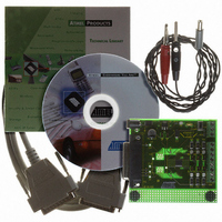
Manufacturer Part Number
ATAB6817
Description
BOARD EVAL FOR T6817
Manufacturer
Atmel
Specifications of ATAB6817
Main Purpose
Power Management, Half H-Bridge Driver (Internal FET)
Embedded
No
Utilized Ic / Part
T6817
Primary Attributes
3 Channel High & Low Side Internal Switch
Secondary Attributes
Graphical User Interface
Processor To Be Evaluated
T6817
Processor Series
T6817
Interface Type
SPI
Maximum Operating Temperature
+ 150 C
Minimum Operating Temperature
- 40 C
Operating Supply Voltage
- 0.3 V to + 40 V
Lead Free Status / RoHS Status
Lead free / RoHS Compliant


8. Electrical Characteristics (Continued)
7.5V < V
10
*) Type means: A =100% tested, B = 100% correlation tested, C = Characterized on samples, D = Design parameter
Note:
5.13
5.14
5.15
5.16
5.17
5.18
No.
6.1
6.2
6.3
6.4
7.1
7.2
7.3
7.4
7.5
8.1
8.2
8.3
6
7
8
VS
Parameters
Open load detection
current
Open load detection
current ratio
Open load detection
threshold
Open load detection
threshold
Output switch on
delay
Output switch off
delay
Inhibit Input
Input voltage low
level threshold
Input voltage high
level threshold
Hysteresis of input
voltage
Pull-down current
Serial Interface – Logic Inputs DI, CLK, CS
Input voltage
low-level threshold
Input voltage
high-level threshold
Hysteresis of input
voltage
Pull-down current pin
DI, CLK
Pull-up current
pin CS
Serial Interface - Logic Output DO
Output voltage low
level
Output voltage high
level
Leakage current
(tri-state)
1. Delay time between rising edge of CS after data transmission and switch on/off output stages to 90% of final level
T6817
< V
OV
(1)
(1)
; 4.5V < V
VCC
< 5.5V; INH = High; –40°C < T
Test Conditions
Input register bit 13
(OLD) = low, output off
Input register bit 13
(OLD) = low, output off
Input register bit 13
(OLD) = low, output off
R
R
V
V
V
I
I
V
0 V < V
OL
OL
INH
DI
CS
CS
Load
Load
, V
= 3 mA
= –2 mA
= 0V
= V
= V
= 1 k
= 1 k
CLK
VCC,
DO
VCC
= V
< V
VCC
VCC
12, 14,
12, 14,
j
8, 15,
< 150°C; unless otherwise specified, all values refer to GND pins.
2, 4
Pin
2-4
2-4
2-4
16
17
16
18
18
18
5
5
5
5
3
Symbol
V
V
I
I
I
V
V
V
HS1–3
LS1–3/
HS1–3
I
I
HS1–3
t
t
LS1–3
V
V
PDSI
PUSI
I
V
I
V
don
doff
DOL
DOH
DO
VS–
PD
V
V
IH
IH
IL
IL
I
I
0.3
0.3
–150
V
V
V
Min.
100
–50
–1V
–10
1.2
0.6
0.6
10
50
VCC
VCC
VCC
2
Typ.
0.7
0.7
Max.
V
V
–30
700
500
0.5
0.5
80
50
–2
10
VCC
VCC
2
2
1
Unit
mV
mV
ms
ms
µA
µA
µA
µA
µA
V
V
V
V
V
V
V
V
4670E–BCD–04/09
Type*
A
A
A
A
A
A
A
A
A
A
A
A
A
A
A
A
A
A
Related parts for ATAB6817
Image
Part Number
Description
Manufacturer
Datasheet
Request
R

Part Number:
Description:
DEV KIT FOR AVR/AVR32
Manufacturer:
Atmel
Datasheet:

Part Number:
Description:
INTERVAL AND WIPE/WASH WIPER CONTROL IC WITH DELAY
Manufacturer:
ATMEL Corporation
Datasheet:
Part Number:
Description:
Low-Voltage Voice-Switched IC for Hands-Free Operation
Manufacturer:
ATMEL Corporation
Datasheet:
Part Number:
Description:
MONOLITHIC INTEGRATED FEATUREPHONE CIRCUIT
Manufacturer:
ATMEL Corporation
Datasheet:
Part Number:
Description:
AM-FM Receiver IC U4255BM-M
Manufacturer:
ATMEL Corporation
Datasheet:
Part Number:
Description:
Monolithic Integrated Feature Phone Circuit
Manufacturer:
ATMEL Corporation
Datasheet:
Part Number:
Description:
Multistandard Video-IF and Quasi Parallel Sound Processing
Manufacturer:
ATMEL Corporation
Datasheet:
Part Number:
Description:
High-performance EE PLD
Manufacturer:
ATMEL Corporation
Datasheet:
Part Number:
Description:
8-bit Flash Microcontroller
Manufacturer:
ATMEL Corporation
Datasheet:
Part Number:
Description:
2-Wire Serial EEPROM
Manufacturer:
ATMEL Corporation
Datasheet: