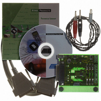
ATAB6817 Atmel, ATAB6817 Datasheet - Page 8

ATAB6817
Manufacturer Part Number
ATAB6817
Description
BOARD EVAL FOR T6817
Manufacturer
Atmel
Specifications of ATAB6817
Main Purpose
Power Management, Half H-Bridge Driver (Internal FET)
Embedded
No
Utilized Ic / Part
T6817
Primary Attributes
3 Channel High & Low Side Internal Switch
Secondary Attributes
Graphical User Interface
Processor To Be Evaluated
T6817
Processor Series
T6817
Interface Type
SPI
Maximum Operating Temperature
+ 150 C
Minimum Operating Temperature
- 40 C
Operating Supply Voltage
- 0.3 V to + 40 V
Lead Free Status / RoHS Status
Lead free / RoHS Compliant
7. Noise and Surge Immunity
Note:
8. Electrical Characteristics
7.5V < V
8
Parameter
Conducted interferences
Interference Suppression
ESD (Human Body Model)
ESD (Machine Model)
*) Type means: A =100% tested, B = 100% correlation tested, C = Characterized on samples, D = Design parameter
Note:
No.
1.1
1.2
1.3
1.4
1.5
2.1
3.1
3.2
3.3
3.4
3.6
3.7
3.8
3.9
1
2
3
VS
1. Test pulse 5: V
Parameters
Current Consumption
Quiescent current
(VS)
Quiescent current
(VCC)
Supply current (VS)
Supply current (VS)
Supply current (VCC)
Internal Oscillator Frequency
Frequency (time
base for delay timers)
Over- and Undervoltage Detection, Power-on Reset
Power-on reset
threshold
Power-on reset delay
time
Undervoltage
detection threshold
Undervoltage
detection hysteresis
Undervoltage
detection delay
Overvoltage
detection threshold
Overvoltage
detection hysteresis
Undervoltage
detection delay
1. Delay time between rising edge of CS after data transmission and switch on/off output stages to 90% of final level
T6817
< V
OV
; 4.5V < V
VCC
Smax
< 5.5V; INH = High; –40°C < T
= 40V
Test Conditions
V
bit SI = low
4.5V < V
INH or bit SI = low
V
operating, all output
stages off,
V
operating, all output
stages on, no load
4.5V < V
normal operating pin
After switching on
V
Input register
bit 14 (SCT) = high
bit 14 (SCT) = low
VS
VS
VS
VCC
< 16V, INH or
< 16V normal
< 16V normal
VCC
VCC
< 5.5V,
< 5.5V,
Test Conditions
ISO 7637–1
VDE 0879 Part 2
MIL-STM 5.1 – 1998
JEDEC EIA / JESD 22 – A115-A
j
< 150°C; unless otherwise specified, all values refer to GND pins.
6, 7
6, 7
6, 7
6, 7
6, 7
6, 7
6, 7
6, 7
Pin
19
19
19
19
Symbol
V
I
I
f
t
V
t
V
t
t
I
VCC
I
I
VCC
OSC
dPor
V
dUV
V
dOV
dOV
VCC
VS
VS
VS
UV
OV
UV
OV
Min.
18.0
1.75
3.4
5.5
19
30
7
7
Typ.
0.8
3.9
0.4
95
1
Max.
22.5
5.25
150
160
1.2
4.4
7.0
40
20
10
45
21
21
Level 4
Level 5
Value
150V
2 kV
Unit
kHz
mA
mA
ms
ms
ms
µA
µA
µA
µs
V
V
V
V
V
4670E–BCD–04/09
(1)
Type*
A
A
A
A
A
A
A
A
A
A
A
A
A
A


