AD9516-4/PCBZ Analog Devices Inc, AD9516-4/PCBZ Datasheet - Page 62
AD9516-4/PCBZ
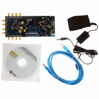
Manufacturer Part Number
AD9516-4/PCBZ
Description
BOARD EVAL FOR AD9516-4 1.8GHZ
Manufacturer
Analog Devices Inc
Specifications of AD9516-4/PCBZ
Main Purpose
Timing, Clock Generator
Embedded
No
Utilized Ic / Part
AD9516-4
Primary Attributes
2 Inputs, 14 Outputs, 1.6GHz VCO
Secondary Attributes
CMOS, LVDS, LVPECL Output Logic, ADIsimCLK™ Graphical User Interface
Silicon Manufacturer
Analog Devices
Application Sub Type
PLL Clock Synthesizer
Kit Application Type
Clock & Timing
Silicon Core Number
AD9516-0, AD9516-1, AD9516-2
Silicon Family Name
AD9516-X
Rohs Compliant
Yes
Lead Free Status / RoHS Status
Lead free / RoHS Compliant


AD9516-4
Reg.
Addr.
(Hex)
0x017
0x018
0x019
0x01A
Bits
[1:0]
[6:5]
4
3
[2:1]
[0]
[7:6]
[5:3]
[2:0]
[6]
Name
Antibacklash
pulse width
Lock detect
counter
Digital lock detect
window
Disable digital
lock detect
VCO cal
divider
VCO cal now
R, A, B counters
SYNC pin reset
R path delay
N path delay
Reference
frequency monitor
threshold
Description
1
0
0
1
1
Required consecutive number of PFD cycles with edges inside lock detect window before the DLD indicates a locked
condition.
6
0
0
1
1
If the time difference of the rising edges at the inputs to the PFD is less than the lock detect window time, the digital lock
detect flag is set. The flag remains set until the time difference is greater than the loss-of-lock threshold.
0: high range (default).
1: low range.
Digital lock detect operation.
0: normal lock detect operation (default).
1: disables lock detect.
VCO calibration divider. Divider used to generate the VCO calibration clock from the PLL reference clock.
2
0
0
1
1
Bit used to initiate the VCO calibration. This bit must be toggled from 0 to 1 in the active registers. To initiate
calibration, use the following three steps: first, ensure that the input reference signal is present; second, set to 0 (if not
zero already), followed by an update bit (Register 0x232, Bit 0); and third, program to 1, followed by another update bit
(Register 0x232, Bit 0).
7
0
0
1
1
R path delay (default = 0x00) (see Table 2).
N path delay (default = 0x00) (see Table 2).
Sets the reference (REF1/REF2) frequency monitor’s detection threshold frequency. This does not affect the VCO
frequency monitor’s detection threshold (see Table 16: REF1, REF2, and VCO Frequency Status Monitor parameter).
0: frequency valid if frequency is above the higher frequency threshold (default).
1: frequency valid if frequency is above the lower frequency threshold.
0
5
0
1
0
1
0
1
0
1
1
0
1
0
1
6
0
1
0
1
Antibacklash Pulse Width (ns)
2.9 (default).
1.3.
6.0.
2.9.
PFD Cycles to Determine Lock
5 (default).
16.
64.
255.
VCO Calibration Clock Divider
2.
4.
8.
16 (default).
Action
Does nothing on SYNC (default).
Asynchronous reset.
Synchronous reset.
Does nothing on SYNC .
Rev. A | Page 62 of 80
Related parts for AD9516-4/PCBZ
Image
Part Number
Description
Manufacturer
Datasheet
Request
R

Part Number:
Description:
IC CLOCK PLL/VCO 2GHZ 64LFCSP
Manufacturer:
Analog Devices Inc
Datasheet:
Part Number:
Description:
IC CLOCK GEN 2.8GHZ VCO 64-LFCSP
Manufacturer:
Analog Devices Inc
Datasheet:
Part Number:
Description:
IC,Fourteen Distributed-Output Clock Driver,LLCC,64PIN,PLASTIC
Manufacturer:
Analog Devices Inc
Datasheet:
Part Number:
Description:
IC,Ten Distributed-Output Clock Driver,LLCC,64PIN,PLASTIC
Manufacturer:
Analog Devices Inc
Datasheet:
Part Number:
Description:
IC,Ten Distributed-Output Clock Driver,LLCC,64PIN,PLASTIC
Manufacturer:
Analog Devices Inc
Datasheet:
Part Number:
Description:
Clock IC With 1.8GHz On-chip VCO
Manufacturer:
Analog Devices Inc
Datasheet:

Part Number:
Description:
BOARD EVAL FOR AD9516-2 2.2GHZ
Manufacturer:
Analog Devices Inc
Datasheet:

Part Number:
Description:
Clock IC With 2.5GHz On-chip VCO EB
Manufacturer:
Analog Devices Inc
Datasheet:
Part Number:
Description:
IC CLOCK GEN 2.8GHZ VCO 64-LFCSP
Manufacturer:
Analog Devices Inc
Datasheet:
Part Number:
Description:
IC,Ten Distributed-Output Clock Driver,LLCC,64PIN,PLASTIC
Manufacturer:
Analog Devices Inc
Datasheet:
Part Number:
Description:
IC,Fourteen Distributed-Output Clock Driver,LLCC,64PIN,PLASTIC
Manufacturer:
Analog Devices Inc
Datasheet:
Part Number:
Description:
IC,Ten Distributed-Output Clock Driver,LLCC,64PIN,PLASTIC
Manufacturer:
Analog Devices Inc
Datasheet:
Part Number:
Description:
Clock IC With 1.8GHz On-chip VCO
Manufacturer:
Analog Devices Inc
Datasheet:
Part Number:
Description:
10/14 Chan Clock IC W/PLL-no VCO
Manufacturer:
Analog Devices Inc
Datasheet:
Part Number:
Description:
10/14 Chan Clock IC W/PLL-no VCO
Manufacturer:
Analog Devices Inc
Datasheet: