STEVAL-ILH001V1 STMicroelectronics, STEVAL-ILH001V1 Datasheet - Page 20
STEVAL-ILH001V1
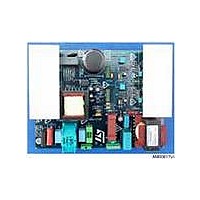
Manufacturer Part Number
STEVAL-ILH001V1
Description
BOARD STF20NM50FD/STF7LITE39BF2
Manufacturer
STMicroelectronics
Specifications of STEVAL-ILH001V1
Design Resources
STEVAL-ILH001V1 Gerber Files STEVAL-ILH001V1 Schematic STEVAL-ILH001V1 Bill of Material
Main Purpose
Lighting, Ballast Control
Embedded
Yes, MCU, 8-Bit
Utilized Ic / Part
L6562, ST7FLITE39F2
Primary Attributes
250W for HID Metal Halide Lamps
Secondary Attributes
PFC, 90 ~ 265 VAC, MCU Based
Product
Power Management Modules
Lead Free Status / RoHS Status
Lead free / RoHS Compliant
Other names
497-8406


Digital interfaces
5.2.1
20/38
Figure 6.
CS is the serial port enable and it is controlled by the SPI master. It goes low at the start of
the transmission and goes back high at the end. SPC is the Serial Port Clock and it is
controlled by the SPI master. It is stopped high when CS is high (no transmission). SDI and
SDO are respectively the serial port data input and output. Those lines are driven at the
falling edge of SPC and should be captured at the rising edge of SPC.
Both the Read Register and Write Register commands are completed in 16 clock pulses or
in multiple of 8 in case of multiple bytes read/write. Bit duration is the time between two
falling edges of SPC. The first bit (bit 0) starts at the first falling edge of SPC after the falling
edge of CS while the last bit (bit 15, bit 23, ...) starts at the last falling edge of SPC just
before the rising edge of CS.
bit 0: RW bit. When 0, the data DI(7:0) is written into the device. When 1, the data DO(7:0)
from the device is read. In latter case, the chip will drive SDO at the start of bit 8.
bit 1: MS bit. When 0, the address will remain unchanged in multiple read/write commands.
When 1, the address is auto incremented in multiple read/write commands.
bit 2-7: address AD(5:0). This is the address field of the indexed register.
bit 8-15: data DI(7:0) (write mode). This is the data that is written into the device (MSb first).
bit 8-15: data DO(7:0) (read mode). This is the data that is read from the device (MSb first).
In multiple read/write commands further blocks of 8 clock periods will be added. When MS
bit is ‘0’ the address used to read/write data remains the same for every block. When MS bit
is ‘1’ the address used to read/write data is increased at every block.
The function and the behavior of SDI and SDO remain unchanged.
SPI read
Figure 7.
SDO
SPC
SDI
CS
SDO
SPC
Read and write protocol
SPI read protocol
SDI
CS
RW
MS
RW
AD5 AD4 AD3 AD2 AD1 AD0
MS
AD5 AD4 AD3 AD2 AD1 AD0
Doc ID 15101 Rev 4
DO7 DO6 DO5 DO4 DO3 DO2 DO1 DO0
DI7 DI6 DI5 DI4 DI3 DI2 DI1 DI0
DO7 DO6 DO5 DO4 DO3 DO2 DO1 DO0
LIS331DLF
Related parts for STEVAL-ILH001V1
Image
Part Number
Description
Manufacturer
Datasheet
Request
R

Part Number:
Description:
BOARD EVAL FOR MEMS SENSORS
Manufacturer:
STMicroelectronics
Datasheet:

Part Number:
Description:
KIT DEV STARTER ST10F276Z5
Manufacturer:
STMicroelectronics
Datasheet:

Part Number:
Description:
BOARD EVAL HDMI $ VIDEO SWITCH
Manufacturer:
STMicroelectronics
Datasheet:

Part Number:
Description:
BOARD DEMO ACCELEROMETER DIL24
Manufacturer:
STMicroelectronics
Datasheet:

Part Number:
Description:
BOARD STLM75/STDS75/ST72F651
Manufacturer:
STMicroelectronics
Datasheet:

Part Number:
Description:
EVAL BOARD 3AXIS MEMS ACCELLRMTR
Manufacturer:
STMicroelectronics
Datasheet:

Part Number:
Description:
BOARD EVAL 8BIT MICRO + TDE1708
Manufacturer:
STMicroelectronics
Datasheet:

Part Number:
Description:
EVAL BOARD A/D TS4657
Manufacturer:
STMicroelectronics
Datasheet:

Part Number:
Description:
BOARD ADAPTER 20DIP LIS3LV02DL
Manufacturer:
STMicroelectronics
Datasheet:

Part Number:
Description:
BOARD DEMO STM8S207R6/LIS331DLH
Manufacturer:
STMicroelectronics
Datasheet:

Part Number:
Description:
STMicroelectronics [RIPPLE-CARRY BINARY COUNTER/DIVIDERS]
Manufacturer:
STMicroelectronics
Datasheet:
Part Number:
Description:
STMicroelectronics [LIQUID-CRYSTAL DISPLAY DRIVERS]
Manufacturer:
STMicroelectronics
Datasheet:
Part Number:
Description:
BOARD EVAL FOR MEMS SENSORS
Manufacturer:
STMicroelectronics
Datasheet: