NCV7708AGEVB ON Semiconductor, NCV7708AGEVB Datasheet - Page 4
NCV7708AGEVB
Manufacturer Part Number
NCV7708AGEVB
Description
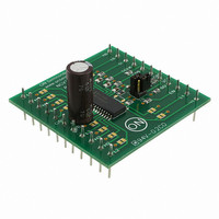
EVAL BOARD FOR NCV7708AG
Manufacturer
ON Semiconductor
Specifications of NCV7708AGEVB
Design Resources
NCV7708 EVB BOM NCV7708GEVB Gerber Files NCV7708 EVB Schematic
Main Purpose
Power Management, Half H-Bridge Driver (Internal FET)
Embedded
No
Utilized Ic / Part
NCV7708
Primary Attributes
6 Channel High & Low Side Internal Switch
Secondary Attributes
SPI Interface
Silicon Manufacturer
On Semiconductor
Silicon Core Number
NCV7708A
Kit Application Type
Driver - Bridge
Application Sub Type
Half Bridge Driver
Development Tool Type
Hardware - Eval/Demo Board
Rohs Compliant
No
Lead Free Status / RoHS Status
Lead free / RoHS Compliant
For Use With/related Products
NCV7708AG
Other names
NCV7708AGEVBOS


Stresses exceeding Maximum Ratings may damage the device. Maximum Ratings are stress ratings only. Functional operation above the
Recommended Operating Conditions is not implied. Extended exposure to stresses above the Recommended Operating Conditions may affect
device reliability.
1. 1−oz copper, 240 mm
2. 1−oz copper, 986 mm
MAXIMUM RATINGS
SOIC 28−pin Package
Junction−to−Lead (psi−JL8, Y
Junction−to−Ambient (R
Power Supply Voltage (VS1, VS2)
Output Pin OUTHx
Output Pin OUTLx
Pin Voltage (Logic Input pins, SI, SCLK, CSB, SO, EN, V
Output Current (OUTL1, OUTL2, OUTL3, OUTL4, OUTL5, OUTL6, OUTH1, OUTH2, OUTH3, OUTH4,
OUTH5, OUTH6)
Electrostatic Discharge, Human Body Model, VS1, VS2, OUTx
Electrostatic Discharge, Human Body Model, all other pins
Electrostatic Discharge, Machine Model
Operating Junction Temperature
Storage Temperature Range
Moisture Sensitivity Level
Electrostatic Discharge, Charged Device Model
(DC)
(AC), t < 500 ms, Ivsx > −2 A
(DC)
(AC – inductive clamping)
(DC)
(AC), t < 500 ms, IOUTLx > −2 A
(AC Inductive Clamping)
(DC) Vds = 12 V
(DC) Vds = 20 V
(DC) Vds = 40 V
(AC) Vds = 12 V, (50 ms pulse, 1 s period)
(AC) Vds = 20 V, (50 ms pulse, 1 s period)
(AC) Vds = 40 V, (50 ms pulse, 1 s period)
MAX 235°C Processing
qJA
2
2
copper area, 0.062″ thick FR4.
copper area, 0.062″ thick FR4.
Thermal Parameters
, q
JA
JL8
)
) or Pins 6−9, 20−23
Rating
CC
http://onsemi.com
)
4
min−pad board
(Note 1)
10
73
Test Conditions
Typical Value
1″−pad board
(Note 2)
11
56
−0.25 to 0.25
−0.3 to 7.0
−1.5 to 1.5
−0.7 to 0.7
−2.0 to 2.0
−0.9 to 0.9
−0.3 to 0.3
−40 to 150
−55 to 150
−0.3 to 40
−0.3 to 40
−0.3 to 34
Value
−1.0
−8.0
−1.0
200
4.0
2.0
1.0
48
3
°C/W
°C/W
Unit
kV
kV
kV
°C
°C
V
V
V
V
A
V
−
Related parts for NCV7708AGEVB
Image
Part Number
Description
Manufacturer
Datasheet
Request
R

Part Number:
Description:
The NCV7708A is a fully protected Hex Half Bridge Driver designed specifically for automotive and industrial motion control applications. The six low and high side drivers are freely configurable and can be controlled separately. This allows for high
Manufacturer:
ON Semiconductor
Datasheet:
Part Number:
Description:
The NCV7708 is a fully protected Hex Half Bridge Driver designed specifically for automotive and industrial motion control applications. The six low and high side drivers are freely configurable and can be controlled separately. This allows for high
Manufacturer:
ON Semiconductor
Datasheet:
Part Number:
Description:
ON Semiconductor [VOLTAGE REGULATOR]
Manufacturer:
ON Semiconductor
Datasheet:
Part Number:
Description:
357-036-542-201 CARDEDGE 36POS DL .156 BLK LOPRO
Manufacturer:
ON Semiconductor
Datasheet:
Part Number:
Description:
357-036-542-201 CARDEDGE 36POS DL .156 BLK LOPRO
Manufacturer:
ON Semiconductor
Datasheet:
Part Number:
Description:
357-036-542-201 CARDEDGE 36POS DL .156 BLK LOPRO
Manufacturer:
ON Semiconductor
Datasheet:
Part Number:
Description:
357-036-542-201 CARDEDGE 36POS DL .156 BLK LOPRO
Manufacturer:
ON Semiconductor
Datasheet:
Part Number:
Description:
357-036-542-201 CARDEDGE 36POS DL .156 BLK LOPRO
Manufacturer:
ON Semiconductor
Datasheet:
Part Number:
Description:
357-036-542-201 CARDEDGE 36POS DL .156 BLK LOPRO
Manufacturer:
ON Semiconductor
Datasheet:
Part Number:
Description:
357-036-542-201 CARDEDGE 36POS DL .156 BLK LOPRO
Manufacturer:
ON Semiconductor
Datasheet:
Part Number:
Description:
357-036-542-201 CARDEDGE 36POS DL .156 BLK LOPRO
Manufacturer:
ON Semiconductor
Datasheet:
Part Number:
Description:
357-036-542-201 CARDEDGE 36POS DL .156 BLK LOPRO
Manufacturer:
ON Semiconductor
Datasheet:
Part Number:
Description:
357-036-542-201 CARDEDGE 36POS DL .156 BLK LOPRO
Manufacturer:
ON Semiconductor
Datasheet:
Part Number:
Description:
Manufacturer:
ON Semiconductor
Datasheet: