74LVC2G66EVB NXP Semiconductors, 74LVC2G66EVB Datasheet - Page 5
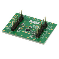
74LVC2G66EVB
Manufacturer Part Number
74LVC2G66EVB
Description
BOARD EVALUATION FOR 74LVC2G66
Manufacturer
NXP Semiconductors
Specifications of 74LVC2G66EVB
Main Purpose
Interface, Analog Switch
Embedded
No
Utilized Ic / Part
74LVC2G66
Primary Attributes
Dual SPST Analog Switch
Secondary Attributes
1.65 ~ 5.5 V Supply
Lead Free Status / RoHS Status
Lead free / RoHS Compliant
Other names
568-5081


NXP Semiconductors
9. Recommended operating conditions
Table 6.
[1]
[2]
[3]
10. Static characteristics
Table 7.
At recommended operating conditions; voltages are referenced to GND (ground = 0 V).
74LVC2G66
Product data sheet
Symbol
V
V
V
T
Δt/ΔV
Symbol Parameter
V
V
I
I
I
I
ΔI
I
S(OFF)
S(ON)
CC
amb
CC
I
SW
IH
IL
CC
To avoid sinking GND current from terminal nZ when switch current flows in terminal nY, the voltage drop across the bidirectional switch
must not exceed 0.4 V. If the switch current flows into terminal nZ, no GND current will flow from terminal nY. In this case, there is no
limit for the voltage drop across the switch.
For overvoltage tolerant switch voltage capability, refer to 74LVCV2G66.
Applies to control signal levels.
HIGH-level
input voltage
LOW-level
input voltage
input leakage
current
OFF-state
leakage
current
ON-state
leakage
current
supply current
additional
supply current
Operating conditions
Static characteristics
Parameter
supply voltage
input voltage
switch voltage
ambient temperature
input transition rise and fall rate
Conditions
V
V
V
V
V
V
V
V
pin nE; V
V
V
V
V
V
pin nE; V
V
V
V
CC
CC
CC
CC
CC
CC
CC
CC
CC
CC
I
SW
CC
SW
CC
CC
= 5.5 V or GND;
= 1.65 V to 1.95 V
= 2.3 V to 2.7 V
= 2.7 V to 3.6 V
= 4.5 V to 5.5 V
= 1.65 V to 1.95 V
= 2.3 V to 2.7 V
= 2.7 V to 3.6 V
= 4.5 V to 5.5 V
= 0 V to 5.5 V
= 5.5 V; see
= 1.65 V to 5.5 V
= 5.5 V
= GND or V
= GND or V
= 5.5 V; see
I
I
= 5.5 V or GND;
= V
CC
All information provided in this document is subject to legal disclaimers.
CC
CC
− 0.6 V;
Figure 8
Figure 9
;
;
Conditions
V
V
Rev. 5 — 16 June 2010
CC
CC
= 1.65 V to 2.7 V
= 2.7 V to 5.5 V
[2]
[2]
[2]
[2]
[2]
0.65 × V
0.7 × V
Min
1.7
2.0
-
-
-
-
-
-
-
-
-
−40 °C to +85 °C
CC
CC
Typ
±0.1
±0.1
±0.1
0.1
5
-
-
-
-
-
-
-
-
[1]
0.35 × V
0.3 × V
Max
500
0.7
0.8
±5
±5
±5
10
-
-
-
-
[1][2]
CC
CC
[3]
[3]
Min
1.65
0
0
−40
-
-
0.65 × V
0.7 × V
−40 °C to +125 °C
74LVC2G66
Min
1.7
2.0
-
-
-
-
-
-
-
-
-
CC
CC
© NXP B.V. 2010. All rights reserved.
Max
5.5
5.5
V
+125
20
10
Bilateral switch
CC
0.35 × V
0.3 × V
±100
±200
±200
5000
Max
200
0.7
0.8
-
-
-
-
CC
CC
Unit
V
V
V
°C
ns/V
ns/V
5 of 26
Unit
V
V
V
V
V
V
V
V
μA
μA
μA
μA
μA
Related parts for 74LVC2G66EVB
Image
Part Number
Description
Manufacturer
Datasheet
Request
R

Part Number:
Description:
IC TRANSCVR TRI-ST DL 24SOIC
Manufacturer:
NXP Semiconductors
Datasheet:

Part Number:
Description:
IC ADDRESS/CLK DRIVER 56-TSSOP
Manufacturer:
IDT, Integrated Device Technology Inc
Datasheet:

Part Number:
Description:
IC MUX/DEMUX 2X1 6TSOP
Manufacturer:
NXP Semiconductors
Datasheet:

Part Number:
Description:
IC SWITCH QUAD SPST 14SOIC
Manufacturer:
NXP Semiconductors
Datasheet:

Part Number:
Description:
IC BUFF DVR TRI-ST 16BIT 48TSSOP
Manufacturer:
IDT, Integrated Device Technology Inc
Datasheet:

Part Number:
Description:
IC BUFF HEX OPEN DRAIN 14TSSOP
Manufacturer:
NXP Semiconductors
Datasheet:
Part Number:
Description:
IC BUFF HEX OPEN DRAIN 14SOICN
Manufacturer:
NXP Semiconductors
Datasheet:
Part Number:
Description:
IC BUFF DVR TRI-ST QD 14SSOP
Manufacturer:
NXP Semiconductors
Datasheet:
Part Number:
Description:
IC BUFF DVR TRI-ST QD 14SOICN
Manufacturer:
NXP Semiconductors
Datasheet:
Part Number:
Description:
IC BUFF DVR TRI-ST QD 14SOICN
Manufacturer:
NXP Semiconductors
Datasheet:
Part Number:
Description:
IC BUFF DVR TRI-ST QD 14SSOP
Manufacturer:
NXP Semiconductors
Datasheet:
Part Number:
Description:
IC BUFF DVR TRI-ST QD 14TSSOP
Manufacturer:
NXP Semiconductors
Datasheet:

Part Number:
Description:
IC BUFF/DVR TRI-ST DUAL 20SSOP
Manufacturer:
NXP Semiconductors
Datasheet:

Part Number:
Description:
IC BUFF/DVR TRI-ST DUAL 20SOIC
Manufacturer:
NXP Semiconductors
Datasheet:

Part Number:
Description:
IC BUFF/DVR TRI-ST DUAL 20TSSOP
Manufacturer:
NXP Semiconductors
Datasheet: