74LVC2G66EVB NXP Semiconductors, 74LVC2G66EVB Datasheet - Page 7
74LVC2G66EVB
Manufacturer Part Number
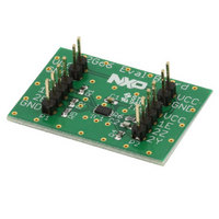
74LVC2G66EVB
Description
BOARD EVALUATION FOR 74LVC2G66
Manufacturer
NXP Semiconductors
Specifications of 74LVC2G66EVB
Main Purpose
Interface, Analog Switch
Embedded
No
Utilized Ic / Part
74LVC2G66
Primary Attributes
Dual SPST Analog Switch
Secondary Attributes
1.65 ~ 5.5 V Supply
Lead Free Status / RoHS Status
Lead free / RoHS Compliant
Other names
568-5081


NXP Semiconductors
Table 8.
At recommended operating conditions; voltages are referenced to GND (ground 0 V); for graphs see
[1]
[2]
74LVC2G66
Product data sheet
Symbol
R
R
R
ON(peak)
ON(rail)
ON(flat)
Typical values are measured at T
Flatness is defined as the difference between the maximum and minimum value of ON resistance measured at identical V
temperature.
Parameter
ON resistance
(peak)
ON resistance
(rail)
ON resistance
(flatness)
ON resistance
10.2 ON resistance
Conditions
V
V
V
V
I
I
I
I
I
V
I
I
I
I
I
V
I
I
I
I
I
V
I
I
I
I
I
V
I
I
I
I
= GND to V
= GND; see
= V
= GND to V
SW
SW
SW
SW
SW
SW
SW
SW
SW
SW
SW
SW
SW
SW
SW
SW
SW
SW
SW
SW
CC
CC
CC
CC
amb
CC
= 4 mA;
= 8 mA; V
= 12 mA; V
= 24 mA; V
= 32 mA; V
= 4 mA;
= 8 mA; V
= 12 mA; V
= 24 mA; V
= 32 mA; V
= 4 mA;
= 8 mA; V
= 12 mA; V
= 24 mA; V
= 32 mA; V
= 4 mA;
= 8 mA; V
= 12 mA; V
= 24 mA; V
= 32 mA; V
= 1.65 V to 1.95 V
= 1.65 V to 1.95 V
= 1.65 V to 1.95 V
= 1.65 V to 1.95 V
= 25 °C and nominal V
; see
All information provided in this document is subject to legal disclaimers.
Figure 10
CC
CC
Figure 10
CC
CC
CC
CC
; see
CC
CC
CC
CC
CC
CC
CC
CC
CC
CC
CC
CC
= 2.3 V to 2.7 V
= 2.3 V to 2.7 V
= 2.3 V to 2.7 V
= 2.3 V to 2.7 V
= 2.7 V
= 3.0 V to 3.6 V
= 4.5 V to 5.5 V
= 2.7 V
= 3.0 V to 3.6 V
= 4.5 V to 5.5 V
= 2.7 V
= 3.0 V to 3.6 V
= 4.5 V to 5.5 V
= 2.7 V
= 3.0 V to 3.6 V
= 4.5 V to 5.5 V
Rev. 5 — 16 June 2010
Figure 10
CC
.
[2]
Min
-
-
-
-
-
-
-
-
-
-
-
-
-
-
-
-
-
-
-
-
−40 °C to +85 °C
Typ
34.0
12.0
10.4
10.4
26.0
7.8
6.2
8.2
7.1
6.9
6.5
5.8
7.6
7.0
6.1
4.9
5.0
3.5
2.0
1.5
[1]
Max
130
30
25
20
15
18
16
14
12
10
30
20
18
15
10
-
-
-
-
-
74LVC2G66
−40 °C to +125 °C
Min
-
-
-
-
-
-
-
-
-
-
-
-
-
-
-
-
-
-
-
-
Figure 11
© NXP B.V. 2010. All rights reserved.
Bilateral switch
Max
195
to
45
38
24
21
45
30
27
30
23
27
18
15
23
15
-
-
-
-
-
CC
Figure
and
7 of 26
Unit
Ω
Ω
Ω
Ω
Ω
Ω
Ω
Ω
Ω
Ω
Ω
Ω
Ω
Ω
Ω
Ω
Ω
Ω
Ω
Ω
16.
Related parts for 74LVC2G66EVB
Image
Part Number
Description
Manufacturer
Datasheet
Request
R

Part Number:
Description:
IC TRANSCVR TRI-ST DL 24SOIC
Manufacturer:
NXP Semiconductors
Datasheet:

Part Number:
Description:
IC ADDRESS/CLK DRIVER 56-TSSOP
Manufacturer:
IDT, Integrated Device Technology Inc
Datasheet:

Part Number:
Description:
IC MUX/DEMUX 2X1 6TSOP
Manufacturer:
NXP Semiconductors
Datasheet:

Part Number:
Description:
IC SWITCH QUAD SPST 14SOIC
Manufacturer:
NXP Semiconductors
Datasheet:

Part Number:
Description:
IC BUFF DVR TRI-ST 16BIT 48TSSOP
Manufacturer:
IDT, Integrated Device Technology Inc
Datasheet:

Part Number:
Description:
IC BUFF HEX OPEN DRAIN 14TSSOP
Manufacturer:
NXP Semiconductors
Datasheet:
Part Number:
Description:
IC BUFF HEX OPEN DRAIN 14SOICN
Manufacturer:
NXP Semiconductors
Datasheet:
Part Number:
Description:
IC BUFF DVR TRI-ST QD 14SSOP
Manufacturer:
NXP Semiconductors
Datasheet:
Part Number:
Description:
IC BUFF DVR TRI-ST QD 14SOICN
Manufacturer:
NXP Semiconductors
Datasheet:
Part Number:
Description:
IC BUFF DVR TRI-ST QD 14SOICN
Manufacturer:
NXP Semiconductors
Datasheet:
Part Number:
Description:
IC BUFF DVR TRI-ST QD 14SSOP
Manufacturer:
NXP Semiconductors
Datasheet:
Part Number:
Description:
IC BUFF DVR TRI-ST QD 14TSSOP
Manufacturer:
NXP Semiconductors
Datasheet:

Part Number:
Description:
IC BUFF/DVR TRI-ST DUAL 20SSOP
Manufacturer:
NXP Semiconductors
Datasheet:

Part Number:
Description:
IC BUFF/DVR TRI-ST DUAL 20SOIC
Manufacturer:
NXP Semiconductors
Datasheet:

Part Number:
Description:
IC BUFF/DVR TRI-ST DUAL 20TSSOP
Manufacturer:
NXP Semiconductors
Datasheet: