74LVC169EVB NXP Semiconductors, 74LVC169EVB Datasheet - Page 2
74LVC169EVB
Manufacturer Part Number
74LVC169EVB
Description
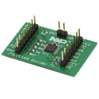
BOARD EVALUATION FOR 74LVC169
Manufacturer
NXP Semiconductors
Specifications of 74LVC169EVB
Main Purpose
Logic, Binary Counter
Embedded
No
Utilized Ic / Part
74LVC169
Primary Attributes
1.2 V ~ 3.6 V Input Voltage
Secondary Attributes
Built-in look-ahead carry capability
Lead Free Status / RoHS Status
Lead free / RoHS Compliant
Other names
568-5082


Circuit schematic of 74LVC169 demo board
The look-ahead carry circuitry is provided for cascading
counters for n-bit synchronous applications without additional
gating. Instrumental in accomplishing this function are two
count-enable (pins CEP and CET) inputs and a terminal
count (pin TC) output. Both count-enable (pins CEP and CET)
inputs must be LOW to count. Input pin CET is fed forward
to enable the terminal count (pin TC) output. Pin TC thus
enabled will produce a LOW-level output pulse with a duration
approximately equal to a HIGH level portion of pin Q0 output.
The LOW level pin TC pulse is used to enable successive
cascaded stages.
Schematics of 74LVC169 demo board are shown in figure
below. A supply voltage of 1.2 to 3.6 V can be used for the
board. In this design, the 74LVC169 is used as a clock divider
that divides the main clock connected to CP pin by 2, 4, 8
and 16. By default, U/D pin is pulled low and PE pin is pulled
HIGH, so counter starts counting down, when clock input edge
goes from LOW to HIGH.
1
2
3
4
5
6
7
8
P1
CLK
D0
D1
D2
D3
CEP
GND
GND
JP1
2
1
The main clock, when connected to the CP pin, is divided by
2 and appears at the Q0 output. There is a clock with 1/4 the
frequency of the main clock at Q1. Clocks with 1/8 and 1/16
of main frequency are available at Q2 and Q3 output pins
respectively.
In order to preset the outputs of the counter to a number
between 0 and its maximum count, the PE pin can be pulled
LOW by using jumper JP1. Data at Dn inputs can now be
loaded to the outputs on next LOW-to-HIGH transition of
main clock. Also, U/D pin can be pulled HIGH by providing
logic high input at pin 1 of P1 connector to count up instead
of counting down. Since CET pin is pulled LOW, when counter
reaches terminal count (HHHH in count up mode and LLLL in
count down mode), TC output, which is normally HIGH, will
go LOW. The low level on TC output can be used to enable
successive cascaded devices
GND
GND
IC1
74LVC169PW
U/D
CP
D0
D1
D2
D3
CEP
GND
GND
VCC
CET
TC
Q0
Q1
Q2
Q3
PE
VCC
C1
0.1uF
GND
NXP SEMICONDU
TITLE:
Document Number:
74LVC169 Evaluation Boar
P2
1
2
3
4
5
6
7
8
VCC
TC
Q0
Q1
Q2
Q3
CET
PE
Related parts for 74LVC169EVB
Image
Part Number
Description
Manufacturer
Datasheet
Request
R

Part Number:
Description:
TXRX 8BIT DUAL CONF VOLT 24TSSOP
Manufacturer:
Fairchild Semiconductor
Datasheet:

Part Number:
Description:
TXRX 8BIT DUAL CONF VOLT 24SOIC
Manufacturer:
Fairchild Semiconductor
Datasheet:

Part Number:
Description:
TXRX 8BIT DUAL CONF VOLT 24QSOP
Manufacturer:
Fairchild Semiconductor
Datasheet:
Part Number:
Description:
TXRX 8BIT DUAL CONF VOLT 24QSOP
Manufacturer:
Fairchild Semiconductor
Datasheet:

Part Number:
Description:
IC SWITCH QUAD 1X2 14TSSOP
Manufacturer:
NXP Semiconductors
Datasheet:

Part Number:
Description:
IC MUX/DEMUX DUAL 4X1 16SSOP
Manufacturer:
NXP Semiconductors
Datasheet:

Part Number:
Description:
IC MUX/DEMUX 8X1 16TSSOP
Manufacturer:
NXP Semiconductors
Datasheet:
Part Number:
Description:
IC MUX/DEMUX DUAL 4X1 16TSSOP
Manufacturer:
NXP Semiconductors
Datasheet:
Part Number:
Description:
IC MUX/DEMUX TRIPLE 2X1 16TSSOP
Manufacturer:
NXP Semiconductors
Datasheet:

Part Number:
Description:
IC MUX/DEMUX 8X1 16SOIC
Manufacturer:
NXP Semiconductors
Datasheet:
Part Number:
Description:
IC MUX/DEMUX 8X1 16SSOP
Manufacturer:
NXP Semiconductors
Datasheet:
Part Number:
Description:
IC MUX/DEMUX DUAL 4X1 16SOIC
Manufacturer:
NXP Semiconductors
Datasheet:
Part Number:
Description:
IC MUX/DEMUX TRIPLE 2X1 16SOIC
Manufacturer:
NXP Semiconductors
Datasheet:
Part Number:
Description:
IC MUX/DEMUX TRIPLE 2X1 16SSOP
Manufacturer:
NXP Semiconductors
Datasheet:

Part Number:
Description:
IC SWITCH QUAD 1X2 14SOIC
Manufacturer:
NXP Semiconductors
Datasheet: