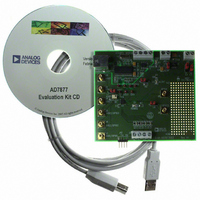
EVAL-AD7877EBZ Analog Devices Inc, EVAL-AD7877EBZ Datasheet - Page 22

EVAL-AD7877EBZ
Manufacturer Part Number
EVAL-AD7877EBZ
Description
BOARD EVALUATION FOR AD7877
Manufacturer
Analog Devices Inc
Datasheets
1.AD7877ACBZ-REEL7.pdf
(44 pages)
2.EVAL-AD7877EBZ.pdf
(16 pages)
3.EVAL-AD7877EBZ.pdf
(44 pages)
Specifications of EVAL-AD7877EBZ
Main Purpose
Interface, Touch Screen Controller
Embedded
No
Utilized Ic / Part
AD7877
Primary Attributes
4-Wire Resistive Touch Screen Controller, SPI Interface, On-Chip: Temp Sensor, Voltage Reference, 8-Bit DAC
Secondary Attributes
USB GUI, LCD Noise Reduction Feature, 2.7 ~ 5.25 V, Wake Up on Touch Feature
Lead Free Status / RoHS Status
Lead free / RoHS Compliant
AD7877
STOPACQ Polarity (Control Register 2, Bit<3>)
This bit should be set according to the polarity of the signal
applied to the STOPACQ pin. If that signal is active high, that
is, no acquisitions should occur during the high period of the
signal, then the POL bit should be set to 1. If the signal is active
low, then the POL bit should be 0. The default value for POL is 0.
First Conversion Delay (Control Register 2, Bits<5:4>)
The first conversion delay (FCD) bits in Control Register 2
program a delay of 500 ns (default), 128 μs, 1.024 ms, or 8.19 ms
before the first conversion, to allow the ADC time to power up.
This delay also occurs before conversion of the X and Y coordi-
nate channels, to allow extra time for screen settling, and after
the last conversion in a sequence, to precharge PENIRQ . If the
signal on the STOPACQ pin is being monitored and goes active
during the FCD, it is ignored until after the FCD period.
Table 8. First Conversion Delay Selection
FCD1
0
0
1
1
Power Management (Control Register 2, Bits<7:6>)
The power management (PM) bits in Control Register 2 allow
the power management features of the ADC to be programmed.
If the PM bits are 00, the ADC is powered down permanently.
This overrides any setting of the mode bits in Control Register 1.
If the PM bits are 01, the ADC and the reference both power
down when the ADC is not converting. If the PM bits are 10,
the ADC and reference are powered up continuously. If the PM
bits are 11, the ADC, but not the reference, powers down when
the ADC is not converting.
Table 9. Power Management Selection
PM1
0
0
1
1
FCD
0
1
0
1
PM0
0
1
0
1
Function
1 clock delay (500 ns)
256 clock delays (128 μs)
2048 clock delays (1.024 ms)
16,384 clock delays (8.19 ms)
Function
Power down continuously (default)
Power down ADC and reference when
ADC is not converting (powers up with
FCD at start of a conversion)
Powered up continuously
Power down ADC when ADC is not
converting (powers up with FCD at start
of conversion)
Rev. B | Page 22 of 44
Acquisition Time (Control Register 2, Bits<9:8>)
The ACQ bits in Control Register 2 allow the selection of
acquisition times for the ADC of 2 μs (default), 4 μs, 8 μs, or
16 μs. The user can program the ADC with an acquisition time
suitable for the type of signal being sampled. For example,
signals with large RC time constants can require longer
acquisition times.
Table 10. Acquisition Time Selection
ACQ1
0
0
1
1
Averaging (Control Register 2, Bits<11:10>)
Signals from touch screens can be extremely noisy. The AVG
bits in Control Register 2 allow multiple conversions to be
performed on each input channel and averaged to reduce noise.
A single conversion can be selected (no averaging), which is the
default, or 4, 8, or 16 conversions can be averaged. Only the
final averaged result is written into the results register.
Table 11. Averaging Selection
AVG1
0
0
1
1
SEQUENCER REGISTERS
There are two sequencer registers on the AD7877. Sequencer
Register 0 controls the measurements performed during a slave
mode sequence. Sequencer Register 1 controls the measure-
ments performed during a master mode sequence.
To include a measurement in a slave mode or master mode
sequence, the relevant bit must be set in Sequencer Register 0 or
Sequencer Register 1. Setting Bit 11 includes a measurement on
ADC Channel 0 in the sequence, which is the Y positional
measurement. Setting Bit 10 includes a measurement on ADC
Channel 1 (X+ measurement), and so on, through Bit 1 for
Channel 10. Figure 37 illustrates the correspondence between
the bits in the sequencer registers and the various measure-
ments. Bit 0 in both sequencer registers is not used. See also the
Detailed Register Descriptions section.
11
Y+
X+
ACQ0
0
1
0
1
AVG0
0
1
0
1
Z2
AUX
1
Figure 37. Sequencer Register
AUX
Function
4 clock periods (2 μs)
8 clock periods (4 μs)
16 clock periods (8 μs)
32 clock periods (16 μs)
Function
ADC performs 1 average per channel
ADC performs 4 averages per channel
ADC performs 8 averages per channel
ADC performs 16 averages per channel
2
AUX
3
BAT
1
BAT
2
TEMP
1
TEMP
2
Z1
USED
NOT
0


