CDB4265 Cirrus Logic Inc, CDB4265 Datasheet - Page 5
CDB4265
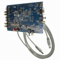
Manufacturer Part Number
CDB4265
Description
BOARD EVAL FOR CS4265 CODEC
Manufacturer
Cirrus Logic Inc
Specifications of CDB4265
Main Purpose
Audio, CODEC
Embedded
No
Utilized Ic / Part
CS4265
Primary Attributes
Stereo, 24-Bit, 192 kHz Sample Rate
Secondary Attributes
Graphic User Interface, S/PDIF/ I2S / I2C / SPI Interface
Description/function
Audio CODECs
Operating Supply Voltage
5 V
Product
Audio Modules
For Use With/related Products
CS4265
Lead Free Status / RoHS Status
Contains lead / RoHS non-compliant
Lead Free Status / RoHS Status
Lead free / RoHS Compliant, Contains lead / RoHS non-compliant
Other names
598-1001


DS657F2
LIST OF FIGURES
12. PACKAGE DIMENSIONS .................................................................................................................. 55
13. THERMAL CHARACTERISTICS AND SPECIFICATIONS ............................................................... 55
14. ORDERING INFORMATION
15. REVISION HISTORY .......................................................................................................................... 56
Figure 1.DAC Output Test Load ................................................................................................................ 12
Figure 2.Maximum DAC Loading .............................................................................................................. 12
Figure 3.Master Mode Serial Audio Port Timing ....................................................................................... 20
Figure 4.Slave Mode Serial Audio Port Timing ......................................................................................... 20
Figure 5.Format 0, Left-Justified up to 24-Bit Data ................................................................................... 21
Figure 6.Format 1, I²S up to 24-Bit Data ................................................................................................... 21
Figure 7.Format 2, Right-Justified 16-Bit Data.
Format 3, Right-Justified 24-Bit Data. ....................................................................................................... 21
Figure 8.Control Port Timing - I²C Format ................................................................................................. 22
Figure 9.Typical Connection Diagram ....................................................................................................... 23
Figure 10.Master Mode Clocking .............................................................................................................. 25
Figure 11.Analog Input Architecture .......................................................................................................... 26
Figure 12.Pseudo-Differential Input Stage ................................................................................................ 27
Figure 13.De-Emphasis Curve .................................................................................................................. 28
Figure 14.Suggested Active-Low Mute Circuit .......................................................................................... 29
Figure 15.Control Port Timing, I²C Write ................................................................................................... 31
Figure 16.Control Port Timing, I²C Read ................................................................................................... 31
Figure 17.De-Emphasis Curve .................................................................................................................. 37
Figure 18.DAC Single-Speed Stopband Rejection ................................................................................... 47
Figure 19.DAC Single-Speed Transition Band .......................................................................................... 47
Figure 20.DAC Single-Speed Transition Band .......................................................................................... 47
Figure 21.DAC Single-Speed Passband Ripple ........................................................................................ 47
Figure 22.DAC Double-Speed Stopband Rejection .................................................................................. 47
Figure 23.DAC Double-Speed Transition Band ........................................................................................ 47
Figure 24.DAC Double-Speed Transition Band ........................................................................................ 48
Figure 25.DAC Double-Speed Passband Ripple ...................................................................................... 48
Figure 26.DAC Quad-Speed Stopband Rejection ..................................................................................... 48
Figure 27.DAC Quad-Speed Transition Band ........................................................................................... 48
Figure 28.DAC Quad-Speed Transition Band ........................................................................................... 48
Figure 29.DAC Quad-Speed Passband Ripple ......................................................................................... 48
Figure 30.ADC Single-Speed Stopband Rejection ................................................................................... 49
Figure 31.ADC Single-Speed Stopband Rejection ................................................................................... 49
Figure 32.ADC Single-Speed Transition Band (Detail) ............................................................................. 49
Figure 33.ADC Single-Speed Passband Ripple ........................................................................................ 49
Figure 34.ADC Double-Speed Stopband Rejection .................................................................................. 49
Figure 35.ADC Double-Speed Stopband Rejection .................................................................................. 49
Figure 36.ADC Double-Speed Transition Band (Detail) ............................................................................ 50
Figure 37.ADC Double-Speed Passband Ripple ...................................................................................... 50
Figure 38.ADC Quad-Speed Stopband Rejection ..................................................................................... 50
Figure 39.ADC Quad-Speed Stopband Rejection ..................................................................................... 50
Figure 40.ADC Quad-Speed Transition Band (Detail) .............................................................................. 50
Figure 41.ADC Quad-Speed Passband Ripple ......................................................................................... 50
11.2 Serial Copy Management System (SCMS) .................................................................................. 53
11.3 Channel Status Data E Buffer Access .......................................................................................... 53
11.1.1 Accessing the E Buffer ........................................................................................................ 53
11.3.1 One-Byte Mode ................................................................................................................... 54
11.3.2 Two-Byte Mode ................................................................................................................... 54
........................................................................................................ 56
CS4265
5
Related parts for CDB4265
Image
Part Number
Description
Manufacturer
Datasheet
Request
R

Part Number:
Description:
Development Kit
Manufacturer:
Cirrus Logic Inc
Datasheet:
Part Number:
Description:
Development Kit
Manufacturer:
Cirrus Logic Inc
Datasheet:


Part Number:
Description:
High-efficiency PFC + Fluorescent Lamp Driver Reference Design
Manufacturer:
Cirrus Logic Inc
Datasheet:
Part Number:
Description:
Development Kit
Manufacturer:
Cirrus Logic Inc
Datasheet:
Part Number:
Description:
Development Kit
Manufacturer:
Cirrus Logic Inc
Datasheet:

Part Number:
Description:
Development Kit
Manufacturer:
Cirrus Logic Inc
Datasheet:
Part Number:
Description:
Development Kit
Manufacturer:
Cirrus Logic Inc
Datasheet:
Part Number:
Description:
Development Kit
Manufacturer:
Cirrus Logic Inc
Datasheet:
Part Number:
Description:
Development Kit
Manufacturer:
Cirrus Logic Inc
Datasheet:

Part Number:
Description:
EVALUATION BOARD FOR CS8427
Manufacturer:
Cirrus Logic Inc
Datasheet:

Part Number:
Description:
BOARD EVAL FOR CS8416 RCVR
Manufacturer:
Cirrus Logic Inc
Datasheet:

Part Number:
Description:
EVALUATION BOARD FOR CS8420
Manufacturer:
Cirrus Logic Inc
Datasheet:

Part Number:
Description:
KIT DEVELOPMENT EP9315 ARM9
Manufacturer:
Cirrus Logic Inc
Datasheet:

Part Number:
Description:
KIT DEVELOPMENT EP9302 ARM9
Manufacturer:
Cirrus Logic Inc
Datasheet: