CDB42448 Cirrus Logic Inc, CDB42448 Datasheet
CDB42448
Specifications of CDB42448


Related parts for CDB42448


CDB42448 Summary of contents
Page 1
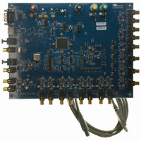
... An auxiliary serial input is available for an additional two channels of PCM data. The CS42448 is available in a 64-pin LQFP package in Commercial (-10°C to +70°C) and Automotive (-40°C to +105°C) grades. The CDB42448 Customer Demonstra- tion board is also available for device evaluation and implementation suggestions. Please refer to Information” ...
Page 2
TABLE OF CONTENTS 1. PIN DESCRIPTIONS 1.1 Digital I/O Pin Characteristics .......................................................................................................... 8 2. TYPICAL CONNECTION DIAGRAM ..................................................................................................... 9 3. CHARACTERISTICS AND SPECIFICATIONS .................................................................................... 10 RECOMMENDED OPERATING CONDITIONS ................................................................................... 10 ABSOLUTE MAXIMUM RATINGS ....................................................................................................... 10 ANALOG INPUT CHARACTERISTICS (COMMERCIAL) .................................................................... ...
Page 3
Power Supply, Grounding, and PCB Layout ................................................................................ 38 5. REGISTER QUICK REFERENCE ........................................................................................................ 39 6. REGISTER DESCRIPTION .................................................................................................................. 41 6.1 Memory Address Pointer (MAP) ..................................................................................................... 41 6.1.1 Increment (INCR) .................................................................................................................. 41 6.1.2 Memory Address Pointer (MAP[6:0]) ..................................................................................... 41 6.2 ...
Page 4
MUTEC Polarity Select (MCPOLARITY) ...................................................................................... 52 6.18 MUTE CONTROL ACTIVE (MUTEC ACTIVE) ............................................................................. 52 7. EXTERNAL FILTERS ........................................................................................................................... 53 7.1 ADC Input Filter .............................................................................................................................. 53 7.1.1 Passive Input Filter ................................................................................................................ 54 7.1.2 Passive Input Filter w/Attenuation ......................................................................................... 54 7.2 ...
Page 5
Figure 37.DSM Transition Band ................................................................................................................ 57 Figure 38.DSM Transition Band (Detail) ................................................................................................... 58 Figure 39.DSM Passband Ripple .............................................................................................................. 58 Figure 40.QSM Stopband Rejection ......................................................................................................... 58 Figure 41.QSM Transition Band ................................................................................................................ 58 Figure 42.QSM Transition Band (Detail) ................................................................................................... 58 Figure 43.QSM ...
Page 6
PIN DESCRIPTIONS AD0/CS AD1/CDIN RST VLC ADC_LRCK VD DGND VLS ADC_SCLK MCLK ADC_SDOUT3 ADC_SDOUT2 ADC_SDOUT1 DAC_SDIN4 DAC_SDIN3 DAC_SDIN2 Pin Name # Address Bit [0]/ Chip Select (Input) - Chip address bit in I²C Mode. Control signal used to select ...
Page 7
DAC_SDIN1 17 DAC_SDIN2 16 DAC Serial Audio Data Input (Input) - Input for two’s complement serial audio data. DAC_SDIN3 15 DAC_SDIN4 14 DAC Serial Clock (Input/Output) - Serial clock for the DAC serial audio interface. Input frequency DAC_SCLK 18 must ...
Page 8
Digital I/O Pin Characteristics Various pins on the CS42448 are powered from separate power supply rails. The logic level for each input should adhere to the corresponding power rail and should not exceed the maximum ratings. Power Pin Name ...
Page 9
TYPICAL CONNECTION DIAGRAM +3 0.1 µ µF 0.1 µF CS5341 A/D Converter CS8416 Receiver S/PDIF optional connection OSC RMCK +1 +5.0 V Digital Audio Processor Micro- Controller ** 2 kΩ 2 ...
Page 10
CHARACTERISTICS AND SPECIFICATIONS RECOMMENDED OPERATING CONDITIONS (AGND = DGND = 0 V, all voltages with respect to ground.) Parameters DC Power Supply Analog Digital Serial Audio Interface Control Port Interface Ambient Temperature Commercial Automotive ABSOLUTE MAXIMUM RATINGS (AGND = ...
Page 11
ANALOG INPUT CHARACTERISTICS (COMMERCIAL) Test Conditions (unless otherwise specified): T scale input sine wave: 1 kHz through the active input filter in surement Bandwidth kHz. Parameter Fs=48 kHz, 96 kHz, 192 kHz Dynamic Range A-weighted ...
Page 12
ANALOG INPUT CHARACTERISTICS (AUTOMOTIVE) Test Conditions (unless otherwise specified): T scale input sine wave: 1 kHz through the active input filter in surement Bandwidth kHz. Parameter Fs=48 kHz, 96 kHz, 192 kHz Dynamic Range A-weighted ...
Page 13
ADC DIGITAL FILTER CHARACTERISTICS Parameter Single-Speed Mode (Note 10) Passband (Frequency Response) Passband Ripple Stopband Stopband Attenuation Total Group Delay Double-Speed Mode (Note 10) Passband (Frequency Response) Passband Ripple Stopband Stopband Attenuation Total Group Delay Quad-Speed Mode (Note 10) Passband ...
Page 14
ANALOG OUTPUT CHARACTERISTICS (COMMERCIAL) Test Conditions (unless otherwise specified): T scale 997 Hz output sine wave (see on page 57; Measurement Bandwidth kHz. Parameter kHz, 96 kHz, 192 kHz Dynamic Range 18 ...
Page 15
ANALOG OUTPUT CHARACTERISTICS (AUTOMOTIVE) Test Conditions (unless otherwise specified): T scale 997 Hz output sine wave (see Bandwidth kHz. Parameter kHz, 96 kHz, 192 kHz Dynamic Range 18 to 24-Bit A-weighted unweighted ...
Page 16
DAC1-4 3.3 µF + AOUTxx R L AGND Figure 2. Output Test Circuit for Maximum Load 16 125 100 75 Analog Output 2 Figure 3. Maximum Loading CS42448 Safe Operating Region ...
Page 17
COMBINED DAC INTERPOLATION & ON-CHIP ANALOG FILTER RESPONSE Parameter Single-Speed Mode Passband (Frequency Response) Frequency Response kHz StopBand StopBand Attenuation Group Delay De-emphasis Error (Note 16) Double-Speed Mode Passband (Frequency Response) Frequency Response ...
Page 18
SWITCHING SPECIFICATIONS - ADC/DAC PORT Inputs: Logic 0 = DGND, Logic 1 = VLS, ADC_SDOUT C Parameters (Note 21) Slave Mode RST pin Low Pulse Width MCLK Frequency MCLK Duty Cycle Input Sample Rate (LRCK) Double-Speed Mode LRCK Duty Cycle ...
Page 19
Notes: 17. After powering up the CS42448, RST should be held low after the power supplies and clocks are settled. 18. See Table 10 on page 43 19. When operating in TDM interface format, VLS is limited to nominal 2.5 ...
Page 20
SWITCHING CHARACTERISTICS - AUX PORT Inputs: Logic 0 = DGND, Logic 1 = VLS. Parameters Master Mode Output Sample Rate (AUX_LRCK) AUX_SCLK Frequency AUX_SCLK Duty Cycle AUX_LRCK Edge to SCLK Rising Edge AUX_SDIN Setup Time Before SCLK Rising Edge AUX_SDIN ...
Page 21
SWITCHING SPECIFICATIONS - CONTROL PORT - I²C MODE VLC = 1 5.0 V, VLS = 5.0 V; Inputs: Logic 0 = DGND, Logic 1 = VLC, SDA C Parameter SCL Clock Frequency ...
Page 22
SWITCHING SPECIFICATIONS - CONTROL PORT - SPI FORMAT VLC = 1 5.0 V, VLS = 5.0 V; Inputs: Logic 0 = DGND, Logic 1 = VLC, CDOUT C Parameter CCLK Clock Frequency ...
Page 23
DC ELECTRICAL CHARACTERISTICS AGND = 0 V; all voltages with respect to ground. Parameters Normal Operation (Note 26) Power Supply Current Power Dissipation Power Supply Rejection Ratio (Note 28) Power-Down Mode (Note 29) Power Dissipation VQ Characteristics Nominal Voltage Output ...
Page 24
APPLICATIONS 4.1 Overview The CS42448 is a highly integrated mixed signal 24-bit audio CODEC comprised of 6 analog-to-digital con- verters (ADC) implemented using multi-bit delta-sigma techniques and 8 digital-to-analog converters (DAC) also implemented using multi-bit delta-sigma techniques. Other functions ...
Page 25
The gain/attenuation of the signal can be adjusted for each AINx independently through the Control (Address 11h-16h)” on page The ADC output data is in 2’s complement binary format. For inputs above positive full scale or below neg- ative full ...
Page 26
Single-Ended Mode is selected using the ADC3_SINGLE bit. Analog input selection is then made via the AINx_MUX bits. See register lections. Refer to Figure 13 on page 29 4.2.3 High-Pass Filter and DC Offset Calibration The high-pass filter continuously subtracts ...
Page 27
Aout bias = ? 3. No audio signal generated. Power-Down (Power Applied Aout = VQ audio signal generated. 4. Control Port Registers reset to default. No Access ...
Page 28
Output Transient Control The CS42448 uses Popguard technology to minimize the effects of output transients during power-up and power-down. This technique eliminates the audio transients commonly produced by single-ended single- supply converters when it is implemented with external DC-blocking ...
Page 29
Line-Level Outputs and Filtering The CS42448 contains on-chip buffer amplifiers capable of producing line-level differential as well as sin- gle-ended outputs on AOUT1-AOUT8. These amplifiers are biased to a quiescent DC level of approxi- mately VQ. The delta-sigma conversion ...
Page 30
De-emphasis is only available in Single-Speed Mode. Please see (DAC_DEM)” on page 46 4.4 System Clocking The CODEC (ADC & DAC) serial audio interface ports operate either as a slave or master. The serial ports accept externally generated clocks in ...
Page 31
CODEC Digital Interface Formats The ADC and DAC serial ports support the I²S, Left-Justified, Right-Justified, One-Line Mode (OLM) and TDM digital interface formats with varying bit depths from shown in clocked out of the ADC ...
Page 32
I²S ADC/DAC_LRCK ADC/DAC_SCLK DAC_SDINx ADC_SDOUTx AOUT AIN 4.5.2 Left-Justified ADC/DAC_LRCK ADC/DAC_SCLK DAC_SDINx ADC_SDOUTx AOUT AIN ...
Page 33
OLM #2 OLM #2 serial audio interface format operates in Single- or Double-Speed Mode and will master or slave ADC/DAC_SCLK at 256Fs. ADC/DAC_LRCK ADC/DAC_SCLK MSB LSB DAC_SDIN1 AOUT1 24 clks AOUT7 DAC_SDIN4 24 clks AIN1 ADC_SDOUT1 24 clks 4.5.6 ...
Page 34
I/O Channel Allocation Digital Input/Output I²S, LJ, RJ DAC_SDIN1 OLM TDM I²S, LJ, RJ DAC_SDIN2 OLM TDM I²S, LJ, RJ DAC_SDIN3 OLM TDM I²S, LJ, RJ DAC_SDIN4 OLM TDM I²S, LJ, RJ ADC_SDOUT1 OLM TDM I²S, LJ, RJ ADC_SDOUT2 ...
Page 35
Left-Justified AUX_LRCK AUX_SCLK AUX_SDIN AUX1 4.7 Control Port Description and Timing The control port is used to access the registers allowing the CS42448 to be configured for ...
Page 36
ADDRESS 1001111 R High Impedance MAP = Memory Address Pointer, 8 bits, MSB first Figure 23. Control Port Timing in SPI ...
Page 37
SCL CHIP ADDRESS (WRITE) SDA AD1 AD0 0 ACK START Since the read operation cannot set the MAP, an aborted write operation is used as a preamble. ...
Page 38
... ADC/DAC_FILT+, VQ pins in order to avoid unwanted coupling into the modulators. The ADC/DAC_FILT+ and VQ decoupling capacitors, particularly the 0.1 µF, must be positioned to mini- mize the electrical path from ADC/DAC_FILT+ and AGND. The CDB42448 evaluation board demonstrates the optimum layout and power supply arrangements. ...
Page 39
REGISTER QUICK REFERENCE Note: The default value in all “Reserved” registers must be preserved. Addr Function 7 01h ID Chip_ID3 Chip_ID2 p 41 default 0 02h Power Con- PDN_ADC3 PDN_ADC2 trol p 42 default 0 03h Functional DAC_FM1 DAC_FM0 ...
Page 40
Addr Function 7 11h Vol. Control AIN1 AIN1 VOL7 p 49 default 0 12h Vol. Control AIN2 AIN2 VOL7 p 50 default 0 13h Vol. Control AIN3 AIN3 VOL7 p 49 default 0 14h Vol. Control AIN4 AIN4 VOL7 p ...
Page 41
REGISTER DESCRIPTION All registers are read/write except for the I.D. and Revision Register and Interrupt Status Register which are read only. See the following bit-definition tables for bit assignment information. The default state of each bit after a power- ...
Page 42
Power Control (Address 02h PDN_ADC3 PDN_ADC2 PDN_ADC1 6.3.1 Power Down ADC Pairs (PDN_ADCX) Default = Disable 1 - Enable Function: When enabled, the respective ADC channel pair (ADC1 - AIN1/AIN2; ADC2 - AIN3/AIN4; and ...
Page 43
Functional Mode (Address 03h DAC_FM1 DAC_FM0 ADC_FM1 6.4.1 DAC Functional Mode (DAC_FM[1:0]) Default = 11 Master Mode 00 - Single-Speed Mode ( kHz sample rates Double-Speed Mode (50 to 100 kHz sample rates) ...
Page 44
MFreq2 MFreq1 Table 11. MCLK Frequency Settings for TDM & OLM Interface Formats 6.5 Interface Formats (Address 04h FREEZE AUX_DIF DAC_DIF2 6.5.1 Freeze Controls (FREEZE) Default = 0 ...
Page 45
DAC_DIF2 DAC_DIF1 6.5.4 ADC Digital Interface Format (ADC_DIF[2:0]) Default = 110 Function: These bits select the digital interface format used for the ADC serial port. The required relationship between the ...
Page 46
ADC3 High Pass Filter Freeze (ADC3_HPF FREEZE) Default = 0 Function: When this bit is set, the internal high-pass filter will be disabled for ADC3.The current DC offset value will be frozen and continue to be subtracted from the ...
Page 47
ADC3 Single-Ended Mode (ADC3 SINGLE) Default = Disabled; Differential input to ADC 1 - Enabled; Single-Ended input to ADC Function: When disabled, this bit removes the 4:2 multiplexer from the signal path of ADC3 allowing a ...
Page 48
Soft Ramp and Zero Cross Control (ADC_SZC[1:0], DAC_SZC[1:0]) Default = Immediate Change 01 - Zero Cross 10 - Soft Ramp 11 - Soft Ramp on Zero Crossings Function: Immediate Change When Immediate Change is selected, all ...
Page 49
Mute ADC Serial Port (MUTE ADC_SP) Default = Disabled 1 - Enabled Function: When enabled, the ADC Serial Port will be muted. 6.8 DAC Channel Mute (Address 07h AOUT8_MUTE AOUT7_MUTE AOUT6_MUTE 6.8.1 Independent Channel ...
Page 50
DAC Channel Invert (Address 10h INV_AOUT8 INV_AOUT7 INV_AOUT6 6.10.1 Invert Signal Polarity (INV_AOUTX) Default = Disabled 1 - Enabled Function: When enabled, these bits will invert the signal polarity of their respective channels. 6.11 ...
Page 51
Status Control (Address 18h Reserved Reserved Reserved 6.13.1 Interrupt Pin Control (INT[1:0]) Default = Active high; high output indicates interrupt condition has occurred 01 - Active low, low output indicates an interrupt condition has ...
Page 52
Status Mask (Address 1Ah Reserved Reserved Reserved Default = 00000 Function: The bits of this register serve as a mask for the error sources found in the register (Read Only)” on page 51 mask ...
Page 53
EXTERNAL FILTERS 7.1 ADC Input Filter The analog modulator samples the input at 6.144 MHz (internal MCLK=12.288 MHz). The digital filter will reject signals within the stopband of the filter. However, there is no rejection for input signals which ...
Page 54
Passive Input Filter The passive filter implementation shown in will not provide optimum source impedance for the ADC modulators. Full analog performance will there- fore not be realized using a passive filter. In this topology the distortion performance is ...
Page 55
Figure 29. Passive Input Filter w/Attenuation DS648F3 ADC1-2 10 μF 2.5 kΩ AIN1+,2+,3+,4+ Ω 2700 pF 2.5 k C0G AIN1-,2-,3-,4- 4.7 μF ADC3 10 μF 2.5 kΩ AIN5A,6A Ω 2700 pF 2.5 k C0G 10 μF 2.5 kΩ AIN5B,6B Ω ...
Page 56
DAC Output Filter Shown below are recommended active and passive output filters. DAC1-4 AOUTx - AOUTx + DAC1-4 AOUTx+ 56 1800 pF 4.75 kΩ 390 pF C0G C0G 5.49 kΩ 2.94 kΩ 887 Ω 1200 pF 1.65 ...
Page 57
ADC FILTER PLOTS Figure 32. SSM Stopband Rejection -10 0.45 0.46 0.47 0.48 0.49 0.5 0.51 Frequency (normalized to Fs) Figure 34. SSM Transition Band (Detail) 0 -10 -20 ...
Page 58
Frequency (normalized to Fs) Figure 38. DSM Transition Band (Detail ...
Page 59
DAC FILTER PLOTS Figure 44. SSM Stopband Rejection Figure 46. SSM Transition Band (detail) Figure 48. DSM Stopband Rejection DS648F3 Figure 45. SSM Transition Band 0.05 0 -0.05 -0. 1 -0.15 -0. 2 -0.25 0 0.05 0.1 0.15 0.2 ...
Page 60
Figure 50. DSM Transition Band (detail) 0 -10 -20 -30 -40 -50 -60 -70 -80 -90 -100 0 0.1 0.2 0.3 0.4 0.5 0.6 Frequency(normalized to Fs) Figure 52. QSM Stopband Rejection 0 -5 -10 -15 -20 -25 -30 -35 ...
Page 61
DEFINITIONS Dynamic Range The ratio of the rms value of the signal to the rms sum of all other spectral components over the specified bandwidth. Dynamic Range is a signal-to-noise ratio measurement over the specified band width made with ...
Page 62
Cirrus Logic, AN18: Layout and Design Rules for Data Converters and Other Mixed Signal Devices, Version 6.0, February 1998. 2. Cirrus Logic, Techniques to Measure and Maximize the Performance of a 120 dB, 96 kHz A/D Converter Integrated ...
Page 63
INFORMATION 64L LQFP PACKAGE DRAWING D D1 DIM MIN A --- A1 0.002 B 0.007 D 0.461 D1 0.390 E 0.461 E1 0.390 e* 0.016 L 0.018 ∝ 0.000° 12.1 Thermal Characteristics Parameter Junction to Ambient Thermal Impedance DS648F3 ...
Page 64
... INFORMATION Product Description 6-in, 8-out CODEC for CS42448 Surround Sound Apps CDB42448 CS42448 Evaluation Board 14.REVISION HISTORY Revision Updated temperature and voltage specifications in the F1 Added test conditions to the Analog Input and Analog Output Characteristics tables. Corrected polarities for pin numbers 31, 32, 38 the ...