CDB42448 Cirrus Logic Inc, CDB42448 Datasheet
CDB42448
Specifications of CDB42448


Related parts for CDB42448


CDB42448 Summary of contents
Page 1
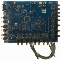
... Input Osc. Cirrus Logic, Inc. www.cirrus.com Description The CDB42448 evaluation board is an excellent means for evaluating the CS42448 CODEC. Evaluation re- quires an analog/digital signal source and analyzer, and power supplies. A Windows must be used to evaluate the CS42448. System timing for the I²S, Left-Justified and Right-Justi- ...
Page 2
... External MCLK Control .................................................................................................... 13 3.5.1 CS5341 MCLK .................................................................................................... 13 3.5.2 TDMer MCLK ...................................................................................................... 13 3.6 Bypass Control - Advanced ............................................................................................. 14 4. FPGA REGISTER QUICK REFERENCE ............................................................................... 15 5. FPGA REGISTER DESCRIPTION ......................................................................................... 16 6. CDB CONNECTORS AND JUMPERS ................................................................................... 28 7. CDB BLOCK DIAGRAM 8. CDB SCHEMATICS 9. CDB LAYOUT ..................................................................................................................... 41 10. REVISION HISTORY ............................................................................................................ 44 2 ................................................................................................... 30 ............................................................................................................. 31 CDB42448 DS648DB2 ...
Page 3
... Figure 21. Bottom side Layer ........................................................................................................ 43 LIST OF TABLES Table 1. Data to SDIN4 ................................................................................................................. 17 Table 2. Data to SDIN3 ................................................................................................................. 17 Table 3. Data to SDIN2 ................................................................................................................. 17 Table 4. Data to SDIN1 ................................................................................................................. 18 Table 5. Clocks to DAC................................................................................................................. 18 Table 6. Clocks to ADC................................................................................................................. 19 Table 7. Data to CS8406............................................................................................................... 19 Table 8. Data to DSP .................................................................................................................... 24 Table 9. System Connections ....................................................................................................... 28 Table 10. Jumper Settings ............................................................................................................ 29 Table 11. Revision History ............................................................................................................ 44 DS648DB2 CDB42448 3 ...
Page 4
... The CDB42448 evaluation board is an excellent means for evaluating the CS42448 CODEC. An- alog and digital audio signal interfaces are provided, an FPGA used for easily configuring the board and a 9-pin serial cable for use with the supplied Windows The CDB42448 schematic set has been partitioned into 10 pages and is shown in Figures 9 through 18. 1.1 Power Power must be supplied to the evaluation board through the +5 ...
Page 5
... External Control Headers The evaluation board has been designed to allow interfacing with external systems via the headers J11 and J25. The 24-pin, 2 row header, J25, provides access to the serial audio signals required to inter- face with a DSP (see Figure 13 on page 35). DS648DB2 CDB42448 5 ...
Page 6
... Serial Control Port A graphical user interface is included with the CDB42448 to allow easy manipulation of the registers in the CS42448 (see the CS42448 data sheet for register descriptions) and FPGA (see section 5 on page 16 for register descriptions). Connecting a cable to the RS-232 con- nector (J7) and launching the Cirrus Logic FlexGUI software will enable the CDB42448. Refer to “ ...
Page 7
... Once the appropriate cable is connected between the CDB42448 and the host PC, load “Flex- Loader.exe” from the CDB42448 directory. Once loaded, all registers are set to their default re- set state. The GUI’s “File” menu provides the ability to save and load script files containing all of the register settings ...
Page 8
... Figure 2. Advanced Register Tab - FPGA CDB42448 DS648DB2 ...
Page 9
... S/PDIF In, S/PDIF Out (SPDIF1-4) This script sets up the CDB42448 to operate the CS8416 as the master and all other de- vices as slave. The CS8416 masters the MCLK bus. Various permutations of this option exist as S/PDIF1, S/PDIF2, S/PDIF3 and S/PDIF4. Each permutation signifies which ADC data is transmitted to the CS8406. ...
Page 10
... CS8416 SCLK CS8416 LRCK FPGA->DAC ADC SCLK ADC LRCK DSP.DAC_SCLK DSP.DAC_LRCK 256Fs SCLK FS FS TDMer 256Fs Figure 3. Internal Sub-Clock Routing CDB42448 CS42448 ADC_MUX[1:0] ADC LRCK ADC_LRCK FPGA->ADC ADC SCLK ADC_SCLK DAC_MUX[1:0] DAC LRCK DAC_LRCK FPGA->DAC DAC SCLK DAC_SCLK ...
Page 11
... DSP OUT2 SDOUT2 CS8416 SDOUT DSP OUT1 DSP OUT3 SDOUT3 CS8416 SDOUT DSP OUT1 DSP OUT4 SDOUT1 ADC1,2,3, AUX TDMer TDM Stream Figure 4. Internal Data Routing CDB42448 CS42448 SDIN1_MUX[1:0] DSPDATA->DAC SDIN1 SDIN1 SDIN2_MUX[1:0] SDIN2 SDIN2 SDIN3_MUX[1:0] SDIN3 SDIN3 SDIN4_MUX[1:0] SDIN4 ...
Page 12
... Clock Selection (T2P/ADC)” on page 20 for implementation). The TDMer is also capable of transmitting the de-multiplexed data to the DSP Header; however, the user must re-time this data using a DSP. The CDB42448 does not provide an option for rout- ing the TDM2PCM clocks to the DSP Header. ...
Page 13
... External MCLK Control Several sources for MCLK exist on the CDB42448. The crystal oscillator, Y1, will master the MCLK bus when no S/PDIF signal is input to the CS8416 (refer to the CS8416 data sheet for details on OMCK operation). This signal will be driven directly out the CS8416. ...
Page 14
... DSP Header DSP_ADC.LRCK/ SCLK DSP_DAC.LRCK/ SCLK DSP.SDOUT1-4 DSP.SDIN1-3 14 FPGA – Bypass Control Register 06h Figure 7. Bypass FPGA Control CDB42448 NOTE: FPGA->ADC/ DACb bits in Reg 03h must be disabled to avoid bus contention. CS42448 ADC.LRCK /SCLK DAC.LRCK /SCLK SDIN1-4 SDOUT1-3 ...
Page 15
... MUX0 MUX2 MUX1 AUX/DAC RST SDOUT->DSP CS5341 DAC->DSP ->AUX DATA_MUX2 DATA_MUX1 DATA_MUX0 FPGA->DAC FPGA->ADC INT.MCLK_ OMCK/DIV_ ‘41_MCLK_ DIV 1.5 CDB42448 Reserved Reserved Reserved ADC.CLK_ ADC.CLK_ MUX1 MUX0 MUX0 128/256 Fs I²S/ M/S 128/256 Fs I²S/ ADC->DSP DSP-> ...
Page 16
... If the CS8416 is selected as the clock source for the P2T converter, this bit is ignored and the CS8416 SDOUT will be selected as the data source for slots 2-4 (see Figure 5 on page 12). 5.1.3 POWER DOWN TDM CONVERTER (PDN_TDMER) Default = Disabled 1- Enabled Function: This bit powers down the TDMer OUT1/OUT4 Reserved CDB42448 Reserved Reserved PDN_TDMer DS648DB2 ...
Page 17
... CS8416 SDOUT 01 DSP SDOUT1 10 DSP SDOUT4 11 ADC_SDOUT1 Table 1. Data to SDIN4 SDIN3.MUX[1:0] Data Selection 00 CS8416 SDOUT 01 DSP SDOUT1 10 DSP SDOUT3 11 ADC_SDOUT3 Table 2. Data to SDIN3 SDIN2.MUX[1:0] Data Selection 00 CS8416 SDOUT 01 DSP SDOUT1 10 DSP SDOUT2 11 ADC_SDOUT2 Table 3. Data to SDIN2 CDB42448 2 1 SDIN2.MUX0 SDIN1.MUX1 SDIN1.MUX0 0 17 ...
Page 18
... This bit toggles a control line for the internal clock buffer to the DAC serial port (see Figure 3 on page 10 SDIN1.MUX[1:0] Data Selection 00 CS8416 SDOUT 01 DSP_ SDOUT1 10 ADC_SDOUT1 11 TDM Stream Table 4. Data to SDIN1 DAC.CLK_ FPGA->DAC MUX0 DAC.CLK_ Clock Selection MUX[1:0] 00 CS8416 01 ADC 10 DSP DAC 11 TDMer Table 5. Clocks to DAC CDB42448 ADC.CLK_ ADC,CLK_ FPGA->ADC- MUX1 MUX0 CODEC DS648DB2 ...
Page 19
... This bit is used to reset the CS8406 and is held low for 300 µs upon FPGA initialization. 5.4.2 DATA MUX(MUX) Default = 100 DS648DB2 ADC.CLK_ Clock Selection MUX[1:0] 00 CS8416 01 DAC 10 DSP ADC 11 TDMer Table 6. Clocks to ADC MUX1 MUX0 MUX[2:0] Data Selection 000 ADC_SDOUT 001 ADC_SDOUT2 010 ADC_SDOUT3 011 ADC_SDOUT1 Table 7. Data to CS8406 CDB42448 128/256 Fs I²S/LJ T2P/ADC 19 ...
Page 20
... Selects the clock source for the CS8406. When de-multiplexing the data on SDOUT1, the CS8406 will need to use the TDMer sub-clocks (see Figure 3 on page 10). 20 MUX[2:0] Data Selection 100 ADC1 (from ADC_SDOUT1) 101 ADC2 (from ADC_SDOUT1) 110 ADC3 (from ADC_SDOUT1) 111 EXT_ADC (from ADC_SDOUT1) Table 7. Data to CS8406 ² S INTERFACE FORMAT (I CDB42448 ² S/LJ) DS648DB2 ...
Page 21
... RMCK/LRCK RATIO SELECT (128/256 FS) Default = 256 128 Fs Function: Selects the RMCK/LRCK ratio for the CS8416. Pin 6 (RST bit) is held low for 300 µs whenever this bit changes. DS648DB2 RST M/S CDB42448 128/256 Fs I²S/LJ RMCK_Master 21 ...
Page 22
... This bit toggles a control line for the external data buffer to route the ADC Data directly to the DSP (see Figure 7 on page 14). The inverted signal controls active low buffers external to the FPGA that 22 ² S INTERFACE FORMAT ( CS5341 DAC->DSP ->AUX CDB42448 ² S/LJ ADC->DSP DSP->DAC DSP->ADC 0 DS648DB2 ...
Page 23
... DSP CLOCKS TO DAC (DSP->DAC) Default = Enable 1 - Disable Function: This bit toggles a control line for the external clock buffer to route the DSP clocks directly to the DAC serial port (see Figure 7 on page 14). 5.6.7 DSP CLOCKS TO ADC (DSP->ADC) Default = Enable 1 - Disable Function: DS648DB2 CDB42448 23 ...
Page 24
... DSP.SDIN2 SDOUT2 ADC2 (from SDOUT1) ADC3 (from SDOUT1) EXT_ADC (from SDOUT1) ADC1 (from SDOUT1) ADC1 (from SDOUT1) ADC2 (from SDOUT1) ADC3 (from SDOUT1) Table 8. Data to DSP CDB42448 2 1 FPGA->DSPDAC FPGA->DSPADC MCLK_M/S DSP.SDIN3 SDOUT3 ADC3 (from SDOUT1) EXT_ADC (from SDOUT1) ...
Page 25
... DSP MCLK (MCLK_M/S) Default = DSP MCLK is a slave to the MCLK bus DSP MCLK masters MCLK bus. Function: Enables/disables the external DSP MCLK output buffer on the MCLK bus. DS648DB2 CDB42448 25 ...
Page 26
... Divide by 2.0 Function: Divides the MCLK from the MCLK bus to the CS5341 by 1 (see Figure 6 on page 13). 5.8.5 LEFT-JUSTIFIED OR I Default = Left Justified ² INT.DIV_ ‘41_MCLK_ DIV 1.5/2 DIV ² S INTERFACE FORMAT (‘41_I CDB42448 ‘41_DIV_ ‘41_I²S/LJ ‘41_RST 1.5/2 ² S/LJ) DS648DB2 ...
Page 27
... RESET (‘41_RST) Default = CS5341 is held in reset 1 - CS5341 is taken out of reset Function: This bit toggles pin 30 of the FPGA and is held low for 300 µs upon FPGA initialization. It will also be held low for 300 µs whenever register 08h[1] changes. DS648DB2 CDB42448 27 ...
Page 28
... RCA phono jacks for analog input signal to CS42448. Input RCA phono jacks for analog input signal to CS5341. Input RCA phono jacks for analog outputs. Output Table 9. System Connections CDB42448 SIGNAL PRESENT 2 C control port signals 2 C control port signals control port signals. ...
Page 29
... Inverted signal from AIN2 input SINGLE IN VA/2 voltage bias *DIFF IN Inverted signal from AIN3 input SINGLE IN VA/2 voltage bias *DIFF IN Inverted signal from AIN4 input SINGLE IN VA/2 voltage bias *A 2-Pole Active Filter P Single-Pole Passive Filter Table 10. Jumper Settings CDB42448 FUNCTION SELECTED *Default factory settings 29 ...
Page 30
... CDB BLOCK DIAGRAM Clocks/Data 30 CDB42448 Data & Clocks ADC/DAC DS648DB2 ...
Page 31
... CDB SCHEMATICS DS648DB2 CDB42448 31 ...
Page 32
... CDB42448 DS648DB2 ...
Page 33
... DS648DB2 CDB42448 33 ...
Page 34
... CDB42448 DS648DB2 ...
Page 35
... DS648DB2 CDB42448 35 ...
Page 36
... CDB42448 DS648DB2 ...
Page 37
... DS648DB2 CDB42448 37 ...
Page 38
... CDB42448 DS648DB2 ...
Page 39
... DS648DB2 CDB42448 39 ...
Page 40
... CDB42448 DS648DB2 ...
Page 41
... CDB LAYOUT DS648DB2 CDB42448 41 ...
Page 42
... CDB42448 DS648DB2 ...
Page 43
... DS648DB2 CDB42448 43 ...
Page 44
... Windows is a registered trademark of Microsoft Corporation. 44 Initial Release Removed Bill of Materials Layer Changes: Corrected silk screen lables for S1, J8, J11 on Figure 19 on page 41. Changed bottom layer lot number on Figure 21 on page 43. Table 11. Revision History CDB42448 Changes DS648DB2 ...