AD7940-DBRD Analog Devices Inc, AD7940-DBRD Datasheet - Page 18
AD7940-DBRD
Manufacturer Part Number
AD7940-DBRD
Description
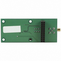
BOARD EVAL FOR AD7940 STAMP SPI
Manufacturer
Analog Devices Inc
Datasheet
1.AD7940BRJZ-REEL7.pdf
(20 pages)
Specifications of AD7940-DBRD
Number Of Adc's
1
Number Of Bits
14
Sampling Rate (per Second)
100k
Data Interface
Serial
Inputs Per Adc
1 Single Ended
Input Range
0 ~ Vdd
Power (typ) @ Conditions
17mW @ 100kSPS & 5 V
Voltage Supply Source
Single Supply
Operating Temperature
-40°C ~ 85°C
Utilized Ic / Part
AD7940
Lead Free Status / RoHS Status
Lead free / RoHS non-compliant


AD7940
For example, if the ADSP-2189 had a 20 MHz crystal, such that
it had a master clock frequency of 40 MHz, the master cycle
time would be 25 ns. If the SCLKDIV register is loaded with the
value 7, then a SCLK of 2.5 MHz is obtained, and 16 master
clock periods will elapse for every 1 SCLK period. Depending
on the throughput rate selected, if the timer register was loaded
with the value 803 (803 + 1 = 804), then 50.25 SCLKs will occur
between interrupts and subsequently between transmit instruc-
tions. This situation will result in nonequidistant sampling since the
transmit instruction is occurring on a SCLK edge. If the number of
SCLKs between interrupts is a whole integer figure of N, then equi-
distant sampling will be implemented by the DSP.
Rev. 0 | Page 18 of 20
AD7940 TO DSP563xx
The connection diagram in Figure 23 shows how the AD7940
can be connected to the ESSI (synchronous serial interface) of
the DSP-563xx family of DSPs from Motorola. Each ESSI (two
on board) is operated in synchronous mode (SYN bit in CRB =
1) with internally generated 1-bit clock period frame sync for
both Tx and Rx (Bits FSL1 = 0 and FSL0 = 0 in CRB). Normal
operation of the ESSI is selected by making MOD = 0 in the
CRB. Set the word length to 16 by setting bits WL1 = 1 and WL0
= 0 in CRA. The FSP bit in the CRB should be set to 1 so that
the frame sync is negative. It should be noted that for signal
processing applications, it is imperative that the frame synchro-
nization signal from the DSP-563xx provide equidistant
sampling.
In the example shown in Figure 23, the serial clock is taken from
the ESSI so the SCK0 pin must be set as an output, SCKD = 1.
*ADDITIONAL PINS OMITTED FOR CLARITY
AD7940*
Figure 23. Interfacing to the DSP-563xx
DOUT
SCLK
CS
SCK
SRD
STD
DSP-563xx*
Related parts for AD7940-DBRD
Image
Part Number
Description
Manufacturer
Datasheet
Request
R

Part Number:
Description:
±1.7g Dual-Axis IMEMS Accelerometer Evaluation Board
Manufacturer:
Analog Devices Inc
Datasheet:

Part Number:
Description:
Inertial Sensor Evaluation System
Manufacturer:
Analog Devices Inc
Datasheet:
Part Number:
Description:
Manufacturer:
Analog Devices Inc
Datasheet:
Part Number:
Description:
Manufacturer:
Analog Devices Inc
Datasheet:
Part Number:
Description:
Manufacturer:
Analog Devices Inc
Datasheet:
Part Number:
Description:
Manufacturer:
Analog Devices Inc
Datasheet:
Part Number:
Description:
Manufacturer:
Analog Devices Inc
Datasheet:
Part Number:
Description:
Manufacturer:
Analog Devices Inc
Datasheet:
Part Number:
Description:
Manufacturer:
Analog Devices Inc
Datasheet:
Part Number:
Description:
Manufacturer:
Analog Devices Inc
Datasheet:
Part Number:
Description:
Manufacturer:
Analog Devices Inc
Datasheet:
Part Number:
Description:
Manufacturer:
Analog Devices Inc
Datasheet:
Part Number:
Description:
Manufacturer:
Analog Devices Inc
Datasheet: