AD7940-DBRD Analog Devices Inc, AD7940-DBRD Datasheet - Page 7
AD7940-DBRD
Manufacturer Part Number
AD7940-DBRD
Description
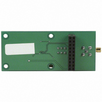
BOARD EVAL FOR AD7940 STAMP SPI
Manufacturer
Analog Devices Inc
Datasheet
1.AD7940BRJZ-REEL7.pdf
(20 pages)
Specifications of AD7940-DBRD
Number Of Adc's
1
Number Of Bits
14
Sampling Rate (per Second)
100k
Data Interface
Serial
Inputs Per Adc
1 Single Ended
Input Range
0 ~ Vdd
Power (typ) @ Conditions
17mW @ 100kSPS & 5 V
Voltage Supply Source
Single Supply
Operating Temperature
-40°C ~ 85°C
Utilized Ic / Part
AD7940
Lead Free Status / RoHS Status
Lead free / RoHS non-compliant


PIN CONFIGURATIONS AND FUNCTION DESCRIPTIONS
Table 5. Pin Function Descriptions
Pin No.
SOT-23
1
2
3
4
5
6
N/A
Pin No.
MSOP
1
2, 3
4
5
7
8
6
GND
Figure 3. SOT-23 Pin Configuration
V
V
DD
IN
1
2
3
Mnemonic
V
GND
V
SCLK
SDATA
CS
NC
DD
IN
(Not to Scale)
AD7940
TOP VIEW
SOT-23
6
5
4
Function
Power Supply Input. The V
Analog Ground. Ground reference point for all circuitry on the AD7940. All analog input signals should
be referred to this GND voltage.
Analog Input. Single-ended analog input channel. The input range is 0 V to V
Serial Clock. Logic input. SCLK provides the serial clock for accessing data from this part. This clock
input is also used as the clock source for the AD7940's conversion process.
Data Out. Logic output. The conversion result from the AD7940 is provided on this output as a serial
data stream. The bits are clocked out on the falling edge of the SCLK input. The data stream from the
AD7940 consists of two leading zeros followed by 14 bits of conversion data that are provided MSB
first. This will be followed by four trailing zeroes if CS is held low for a total of 24 SCLK cycles. See the
Serial Interface section.
Chip Select. Active low logic input. This input provides the dual function of initiating conversions on
the AD7940 and framing the serial data transfer.
No Connect. This pin should be left unconnected.
CS
SDATA
SCLK
Rev. 0 | Page 7 of 20
DD
range for the AD7940 is from 2.5 V to 5.5 V.
GND
GND
V
Figure 4. MSOP Pin Configuration
V
DD
IN
NC = NO CONNECT
1
2
3
4
(Not to Scale)
AD7490
TOP VIEW
MSOP
8
7
6
5
CS
SDATA
NC
SCLK
DD
.
AD7940
Related parts for AD7940-DBRD
Image
Part Number
Description
Manufacturer
Datasheet
Request
R

Part Number:
Description:
±1.7g Dual-Axis IMEMS Accelerometer Evaluation Board
Manufacturer:
Analog Devices Inc
Datasheet:

Part Number:
Description:
Inertial Sensor Evaluation System
Manufacturer:
Analog Devices Inc
Datasheet:
Part Number:
Description:
Manufacturer:
Analog Devices Inc
Datasheet:
Part Number:
Description:
Manufacturer:
Analog Devices Inc
Datasheet:
Part Number:
Description:
Manufacturer:
Analog Devices Inc
Datasheet:
Part Number:
Description:
Manufacturer:
Analog Devices Inc
Datasheet:
Part Number:
Description:
Manufacturer:
Analog Devices Inc
Datasheet:
Part Number:
Description:
Manufacturer:
Analog Devices Inc
Datasheet:
Part Number:
Description:
Manufacturer:
Analog Devices Inc
Datasheet:
Part Number:
Description:
Manufacturer:
Analog Devices Inc
Datasheet:
Part Number:
Description:
Manufacturer:
Analog Devices Inc
Datasheet:
Part Number:
Description:
Manufacturer:
Analog Devices Inc
Datasheet:
Part Number:
Description:
Manufacturer:
Analog Devices Inc
Datasheet: